 ALLPCB


Introduction
Electromagnetic compatibility (EMC) remains a critical challenge in modern PCB design, particularly as operating frequencies increase and board densities rise. Proper grounding techniques, such as via stitching, play a pivotal role in achieving emi reduction pcb and ensuring pcb layout emc compliance. Via stitching connects multiple ground planes across layers, minimizing impedance discontinuities and suppressing radiated emissions. Minimum drill size directly impacts the feasibility of dense via arrays, balancing fabrication limits with performance needs. This article explores these techniques through logical engineering principles, offering structured guidance for electrical engineers. Understanding these elements helps optimize grounding pcb strategies for reliable EMC performance.
What Is Via Stitching and Why It Matters for EMC
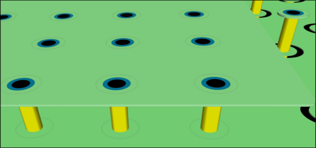
Via stitching involves placing an array of closely spaced vias to interconnect ground planes on different layers of a multilayer PCB. This technique creates low-impedance paths, effectively tying disparate ground regions together and preventing potential differences that lead to noise coupling. In high-speed designs, via stitching emc benefits arise from reduced loop areas and better return current paths, which curb electromagnetic interference. Without adequate stitching, ground bounces can radiate through board edges, failing EMC tests. Minimum drill size constraints influence stitching density, as smaller vias enable tighter spacing without violating fabrication rules. Ultimately, these methods ensure signal integrity while meeting regulatory EMC thresholds.
Engineers often overlook via stitching in early layout stages, leading to costly respins. It serves dual purposes: thermal relief for high-current paths and shielding against crosstalk. For emi reduction pcb, stitching along sensitive traces forms a virtual barrier, containing fields within defined zones. Industry practices emphasize its role in multilayer boards where layer transitions demand robust grounding. Compliance with standards like IPC-2221 reinforces its necessity for controlled impedance environments.
Technical Principles of Via Stitching and Via Fence Design
Via stitching operates on the principle of distributed capacitance and inductance minimization between layers. Each via acts as a short transmission line, with its impedance determined by diameter, plating thickness, and length equal to board thickness. Arrays reduce overall inductance by paralleling multiple paths, lowering ground impedance at high frequencies. For via stitching emc, spacing must be less than one-twentieth of the wavelength at the highest frequency of interest to maintain shielding effectiveness. This creates a continuous ground reference, suppressing common-mode currents that contribute to emissions.
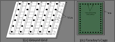
A via fence design extends this concept into a linear or perimeter array, functioning like a picket fence to block slotline modes along edges. Fields attempting to propagate between layers encounter the dense via wall, experiencing high attenuation. The effectiveness depends on via count, spacing, and drill size; tighter fences demand smaller minimum drill sizes for practicality. Grounding pcb through fences prevents edge radiation, a common EMC failure mode in unshielded boards. Parasitic coupling between adjacent vias must be managed to avoid resonances.
In pcb layout emc compliance, these structures mimic solid metal shields but leverage PCB fabrication. Return currents follow the lowest impedance path, staying close to signal traces when stitching is present. Simulations reveal that unstitched splits in ground planes increase emissions by orders of magnitude. Fabricators adhere to aspect ratio limits, typically 10:1 for drill diameter to board thickness, per IPC guidelines.
Minimum Drill Size Considerations for Effective Grounding
Minimum drill size sets the foundation for viable via stitching, as it dictates annular ring requirements and plating uniformity. Mechanical drilling achieves reliable holes down to 0.15 mm, while laser drilling extends to smaller for microvias. Smaller drills enable denser stitching but raise aspect ratio challenges, risking poor plating and higher resistance. IPC-6012 specifications outline minimum annular rings to prevent breakouts, ensuring mechanical strength in Class 3 boards. Engineers must balance drill size with board thickness to maintain via reliability under thermal stress.
For via fence design, minimum drill size influences spacing feasibility; 0.2 mm drills allow λ/20 arrays at GHz frequencies without excessive via count. Oversized drills increase inductance, degrading emi reduction pcb performance. Plating thickness, typically 25 microns, adds to finished hole size, impacting current capacity. Grounding pcb vias under components benefit from minimal sizes to preserve pad space. Fabrication tolerances, such as drill wander, amplify with smaller sizes, demanding precise registration.
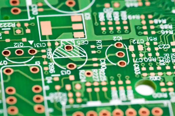
Aspect ratios guide selection: for 1.6 mm boards, 0.15 mm drills approach limits, suitable for stitching but not blind vias. Electrical models treat via arrays as pi-networks, with drill size tuning capacitance. Compliance testing reveals that undersized drills cause intermittent opens post-reflow.
Best Practices for Via Stitching and Via Fence Implementation
Start with solid ground planes on inner layers, dedicating at least one full plane to ground for pcb layout emc compliance. Place stitching vias every 1/10 to 1/20 wavelength along traces carrying fast edges, prioritizing high-speed signals. For perimeter fences, position 3-5 mm from edges, spacing vias at 5-10 mm centers adjusted for frequency. Use 0.2-0.3 mm drills for standard boards, ensuring pads overlap planes adequately. Automate placement in design tools, verifying no splits interrupt stitching paths.
Incorporate stitching near layer transitions and connectors to equalize potentials. Via fence design around analog sections isolates noise from digital domains. Test inductance with 2D field solvers, targeting below 1 nH per via. For emi reduction pcb, combine with guard traces between fences. Avoid over-stitching power planes to prevent capacitance coupling.
Monitor thermal effects; dense stitching aids heat spreading but monitor drill smear. J-STD guidelines support via reliability in assembly processes. Prototype and measure emissions to validate spacing.
Troubleshooting Common Issues in Via Stitching for EMC
Ground loops emerge when stitching misses splits, causing voltage differentials detectable in near-field probes. Solution: flood-fill ground pours and stitch comprehensively. Excessive emissions from edges signal sparse fences; densify to λ/20. Fabrication rejects due to small drills often stem from aspect ratio violations; upscale or thin boards. Post-assembly opens trace to poor plating; inspect with IPC-A-600 criteria.
Crosstalk spikes indicate wide spacing; recalculate based on clock rates. Simulations mismatch reality from unmodeled parasitics; include via stubs. Component ground pads lacking nearby stitching amplify noise; add dedicated vias adjacent.
Conclusion
Via stitching and minimum drill size optimization form cornerstone grounding pcb techniques for EMC success. Dense arrays and fences deliver emi reduction pcb by minimizing impedances and shielding paths. Adhering to IPC standards ensures manufacturability alongside performance. Electrical engineers benefit from structured implementation, from wavelength-based spacing to aspect ratio checks. Prioritizing these in pcb layout emc compliance yields robust designs passing tests first pass. Future high-speed trends demand even finer drills and smarter automation.
FAQs
Q1: What spacing should via stitching use for via stitching emc at 1 GHz?
A1: For 1 GHz signals, wavelength is 300 mm in air, so space vias at 15 mm or less (λ/20) to form an effective barrier. Tighter spacing enhances shielding but increases via count and cost. Verify with simulations for board-specific dielectrics. This practice supports grounding pcb integrity across layers.
Q2: How does minimum drill size affect via fence design?
A2: Smaller drills like 0.15 mm enable denser fences for better emi reduction pcb, but limit to aspect ratios under 10:1. Larger drills simplify fabrication yet raise inductance, weakening high-frequency performance. Balance with annular ring rules from IPC-6012 for reliability. Optimal sizes depend on board thickness.
Q3: Why is via stitching critical for pcb layout emc compliance?
A3: Via stitching ties ground planes, reducing return path inductance and radiated emissions. Without it, layer splits create slots radiating noise. It ensures low-impedance references for signals, aiding compliance. Combine with fences for edge control.
Q4: Can via stitching replace a full ground plane?
A4: No, stitching supplements planes by bridging gaps, not substituting them. Full planes provide broad low-impedance; stitching handles discontinuities. Use both for comprehensive grounding pcb in multilayer boards.
References
IPC-2221B — Generic Standard on the Design of Rigid Printed Boards and Rigid Printed Board Assemblies. IPC, 2003
IPC-6012E — Qualification and Performance Specification for Rigid Printed Boards. IPC, 2017
J-STD-001G — Requirements for Soldered Electrical and Electronic Assemblies. IPC, 2017





