High-frequency PCB manufacturing can be expensive, but it doesn’t have to break your budget. By focusing on smart design choices, material selection, and manufacturing strategies, you can achieve PCB cost reduction while maintaining the performance needed for high-frequency applications like RF, microwave, and 5G systems. In this blog, we’ll dive deep into practical ways to balance performance and cost, covering key factors such as high-frequency PCB cost drivers, material selection cost, layer count cost, and manufacturing tolerances cost. Let’s explore how to optimize your project for efficiency and savings.
Understanding High-Frequency PCBs and Their Cost Challenges
High-frequency printed circuit boards (PCBs) are specialized boards designed to handle signals typically above 1 GHz, used in applications like telecommunications, radar, and satellite systems. These boards require precise engineering to ensure signal integrity, minimal loss, and controlled impedance—often at a higher cost than standard PCBs. The main high-frequency PCB cost drivers include advanced materials, tight manufacturing tolerances, and complex designs with multiple layers.
Unlike standard PCBs, high-frequency designs can’t afford signal degradation, so every aspect, from material choice to trace width, must be carefully planned. However, with the right approach, you can reduce expenses without sacrificing quality. Let’s break down the strategies to achieve cost-effective manufacturing for these advanced boards.
Key Cost Drivers in High-Frequency PCB Manufacturing
Before diving into solutions for PCB cost reduction, it’s important to understand what drives expenses in high-frequency PCB production. Identifying these factors helps you target areas for savings.
1. Material Selection Cost
The choice of substrate material is one of the biggest high-frequency PCB cost drivers. High-frequency signals require materials with low dielectric constant (Dk) and low loss tangent (Df) to minimize signal loss and maintain integrity. Common materials include PTFE-based laminates and specialized ceramics, which are significantly more expensive than standard FR-4 used in low-frequency boards.
For example, FR-4 has a dielectric constant of around 4.5 and is unsuitable for frequencies above 1 GHz due to high signal loss. In contrast, a PTFE-based material might have a Dk of 2.2 and a Df of 0.0009, ensuring better performance at 10 GHz or higher—but at a cost of 5 to 10 times more per square inch. Balancing material selection cost with performance is critical, and we’ll explore affordable alternatives later.
2. Layer Count Cost
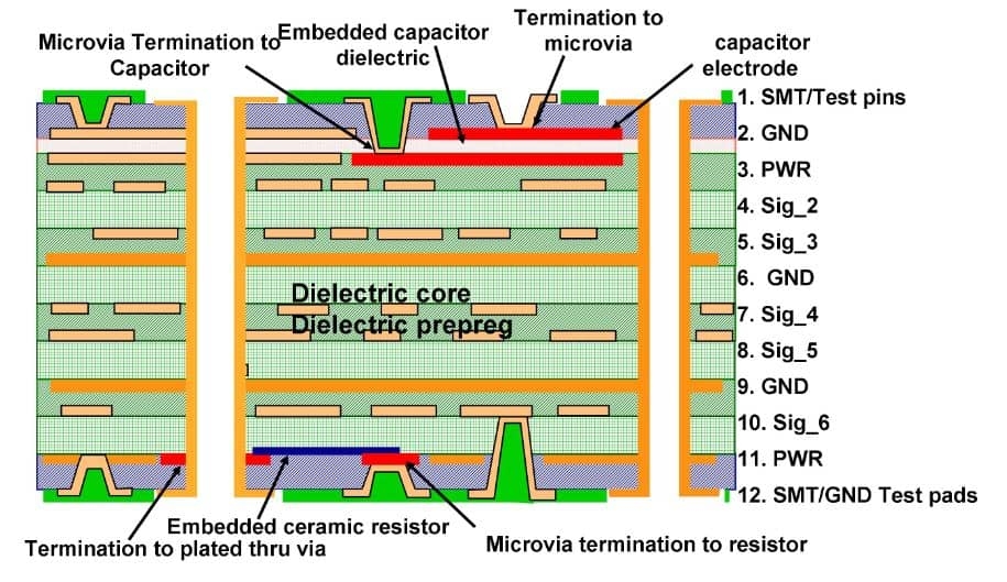
The number of layers in a PCB directly impacts the layer count cost. High-frequency designs often need multiple layers to separate signal and ground planes, reducing interference and crosstalk. However, each additional layer increases material and manufacturing expenses. A 4-layer board might cost 30-50% more than a 2-layer board, and costs escalate further with 6 or 8 layers due to added complexity in alignment and drilling.
3. Manufacturing Tolerances Cost
High-frequency PCBs demand tight manufacturing tolerances cost to maintain consistent impedance (often within ±10% or less) and precise trace widths. For instance, a 50-ohm impedance line might require a trace width of 0.5 mm with a tolerance of ±0.05 mm. Achieving this precision requires advanced equipment and slower production processes, driving up costs by 20-40% compared to standard tolerances.
Strategies for Cost-Effective High-Frequency PCB Manufacturing
Now that we’ve identified the main high-frequency PCB cost drivers, let’s explore actionable strategies to reduce expenses without compromising performance. These tips focus on design optimization, material choices, and manufacturing processes.
1. Optimize Material Selection for Cost and Performance
Choosing the right material doesn’t mean always going for the most expensive option. To manage material selection cost, consider hybrid designs or cost-effective alternatives. For instance, instead of using a full PTFE substrate, you can use a hybrid stack-up with PTFE only on high-frequency signal layers and cheaper FR-4 on power or ground layers. This approach can cut material costs by up to 30% while still achieving a low Dk of around 2.5 on critical layers.
Another option is to select mid-range materials like hydrocarbon ceramic laminates, which offer a Dk of 3.0-3.5 and a Df of 0.003, suitable for frequencies up to 5 GHz. These materials are often 20-40% cheaper than pure PTFE while providing adequate performance for many applications.
2. Minimize Layer Count with Smart Design
Reducing layer count cost starts with efficient design. Use simulation tools to determine the minimum number of layers needed for signal integrity. For example, instead of a 6-layer design, you might achieve the same results with a 4-layer board by optimizing trace routing and ground plane placement. Each layer reduction can save 10-20% on overall board cost.
Additionally, consider using microstrip or stripline configurations strategically. Microstrip (signal traces on outer layers) is cheaper to manufacture than stripline (traces between layers) because it requires less precise alignment, potentially saving 5-10% on production costs.
3. Relax Tolerances Where Possible
While tight tolerances are necessary for critical signal paths, not every part of the board needs the same precision. To lower manufacturing tolerances cost, identify non-critical areas where standard tolerances can be applied. For instance, power lines or non-high-frequency signals can often tolerate ±15% impedance variation without impacting performance. This selective approach can reduce manufacturing costs by 10-15%.
Work closely with your manufacturer to define realistic tolerances. Over-specifying can lead to unnecessary expenses, while under-specifying risks performance issues. Aim for a balance, such as maintaining ±8% impedance on RF lines while allowing ±12% on less critical traces.
4. Simplify Design for Manufacturability
Design for Manufacturability (DFM) principles are essential for PCB cost reduction. Simple changes can make a big difference. For example, avoid unnecessarily small vias or trace widths that require specialized equipment. Standardizing via sizes to 0.3 mm or larger can reduce drilling costs by 5-10% compared to microvias below 0.2 mm.
Also, optimize panelization to minimize material waste. Grouping multiple small boards on a single panel during manufacturing can save up to 15% on material costs. Ensure your design avoids odd shapes or cutouts that complicate production and increase scrap rates.
5. Partner with the Right Manufacturer
Choosing a manufacturer experienced in high-frequency PCB production can save costs in the long run. They can provide guidance on cost-effective materials and processes tailored to your project. Bulk ordering or long-term partnerships can also lead to discounts of 10-20% on production runs. Clear communication about your budget and performance needs ensures they prioritize cost-saving measures without cutting corners on quality.
Balancing Performance and Budget: Practical Examples
Let’s look at a couple of real-world scenarios to see how these strategies apply to high-frequency PCB projects.
Example 1: 5G Antenna Module
For a 5G antenna module operating at 28 GHz, signal integrity is critical. Using a full PTFE substrate would cost $200 per square foot, but a hybrid design with PTFE on signal layers and FR-4 on ground layers reduces this to $120 per square foot—a 40% saving. By limiting the design to 4 layers instead of 6 through optimized routing, an additional 20% cost reduction is achieved. The result is a high-performing board at nearly half the initial material cost.
Example 2: Automotive Radar System
An automotive radar system at 77 GHz requires tight tolerances for impedance control. By relaxing tolerances on non-critical power lines to ±15% while keeping signal lines at ±8%, manufacturing costs drop by 10%. Using a mid-range hydrocarbon laminate instead of premium PTFE saves another 25% on materials, maintaining a low Df of 0.0025 for adequate performance. These combined savings make the project viable within a tight budget.
Additional Tips for PCB Cost Reduction
Beyond the main strategies, here are a few more ways to trim expenses in high-frequency PCB manufacturing:
- Standardize Components: Use widely available components with standard sizes to avoid custom orders, saving 5-10% on assembly costs.
- Prototype Early: Test designs with small prototype runs to catch issues before full production, preventing costly redesigns.
- Optimize Trace Lengths: Shorter traces reduce signal loss and material usage, cutting costs by a small but meaningful 2-5%.
Conclusion: Achieving Cost-Effective High-Frequency PCB Manufacturing
High-frequency PCB manufacturing doesn’t have to be prohibitively expensive. By addressing key high-frequency PCB cost drivers like material selection cost, layer count cost, and manufacturing tolerances cost, you can achieve significant PCB cost reduction without sacrificing performance. Smart material choices, streamlined designs, and close collaboration with manufacturers are the foundation of balancing budget and quality.
Whether you’re working on a 5G system, radar technology, or another high-frequency application, these strategies can help you save 20-40% on production costs while meeting strict performance standards. Start by reviewing your design for optimization opportunities and selecting materials that match your frequency needs without overpaying. With careful planning, cost-effective high-frequency PCB manufacturing is within reach.
 ALLPCB


