ALLPCB


What Is HBM3E Memory?
As AI training datasets continue to grow, accelerators require terabyte-scale memory bandwidth. HBM3E delivers high memory bandwidth and energy efficiency, positioning itself as a preferred memory solution for AI training hardware.
Introduced in January 2022, HBM3 is the latest generation of High Bandwidth Memory (HBM), based on a high-performance 2.5D/3D memory architecture. Like previous generations, HBM3 uses a wide 1024-bit data bus. It operates at 6.4 Gb/s, delivering 819 GB/s of bandwidth. HBM3E extends this to 9.6 Gb/s, offering the same feature set with improved performance. Its high bandwidth, density, and compact footprint make it an ideal memory solution for AI workloads.
What Is a 2.5D/3D Architecture?
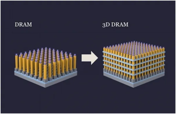
HBM memory consists of 3D-stacked DRAM. The ¡°2.5D¡± designation refers to how HBM devices are connected to processors such as GPUs or AI accelerators. Each HBM device requires approximately 1024 signal lines to connect to the processor, and with additional lines for commands, addresses, and clock signals, the total can reach about 1700¡ªfar beyond what a standard PCB can support.
To accommodate this, a silicon interposer is used as an intermediary. Much like integrated circuits, signal lines can be etched into the interposer, allowing for the dense wiring needed by the HBM interface. Both the HBM memory and processor are mounted on top of this interposer, forming the 2.5D architecture.
How HBM3E Differs from HBM2E, HBM2, and HBM
HBM3 represents the third generation of the HBM standard. Each generation has seen increases in data rate, stack height, and DRAM chip density¡ªresulting in greater bandwidth and capacity. The original HBM offered 1 Gb/s speeds and up to 16 GB in 8-high stacks. HBM3 increases speed to 6.4 Gb/s and supports 32 GB in 16-high stacks. HBM3E takes this further, boosting the data rate to 9.6 Gb/s.
As HBM density improves, chip architects are also designing accelerators and GPUs with higher connectivity. For instance, systems featuring six HBM3 devices at 6.4 Gb/s can achieve memory bandwidths of up to 4.9 TB/s.
Additional Advances in HBM3E and HBM3
HBM3 and HBM3E also introduce improvements in power, memory access, and reliability, availability, and serviceability (RAS).
Power Efficiency
HBM3/3E reduces core voltage from 1.2V (in HBM2E) to 1.1V, and IO signal voltage to 400mV. Lower voltages reduce overall power consumption, helping to offset the increased power demands of higher data rates.
Channel Architecture
HBM3E/3 divides the 1024-bit bus into 16¡Á64-bit channels or 32¡Á32-bit pseudo channels. This is a significant increase over HBM2E¡¯s 8¡Á128-bit channels and 16¡Á64-bit pseudo channels, effectively doubling the number of channels and improving performance.
RAS Enhancements
New features include additional host- and device-side ECC (error correction code), support for Refresh Management (RFM), and Adaptive Refresh Management (ARFM), all contributing to greater reliability and maintainability.
Rambus HBM3E/3 Memory Controller Core
The Rambus HBM3E/3 memory controller core is optimized for high bandwidth and low latency, delivering maximum performance and flexibility for AI training within a compact and energy-efficient package.
This controller pushes data rates to a market-leading 9.6 Gb/s per data pin¡ªsignificantly above the standard 6.4 Gb/s. The interface supports 16 independent channels of 64 bits each, totaling a 1024-bit wide bus. At full speed, this enables up to 1,229 GB/s (1.23 TB/s) of memory bandwidth per HBM3E/3 device.
Conclusion
HBM delivers unmatched memory bandwidth in a compact, high-capacity form factor, making it the memory of choice for AI/ML and other high-performance computing workloads. HBM3 raises data rates to 6.4 Gb/s with further scalability expected. The Rambus HBM3E/3 controller core supports this evolution with industry-leading performance up to 9.6 Gb/s, enabling designers to achieve up to 1.23 TB/s per connected HBM3E/3 device.