ALLPCB


Introduction
In the realm of advanced electronics, 8-layer printed circuit boards represent a critical step up in complexity and performance from simpler designs. These multilayer boards enable high-density routing, better signal integrity, and enhanced power distribution, making them essential for applications like telecommunications equipment, automotive systems, and data processing units. However, the 8-layer PCB manufacturing cost can vary widely based on design choices and production parameters. Engineers must grasp these cost drivers to optimize budgets without compromising reliability. This article breaks down the key elements influencing 8-layer PCB material cost, fabrication cost, assembly cost, and strategies for cost-effective 8-layer PCB design. By understanding these factors, technical teams can make informed decisions aligned with project needs.
What Is an 8-Layer PCB and Why It Matters for Electrical Engineers
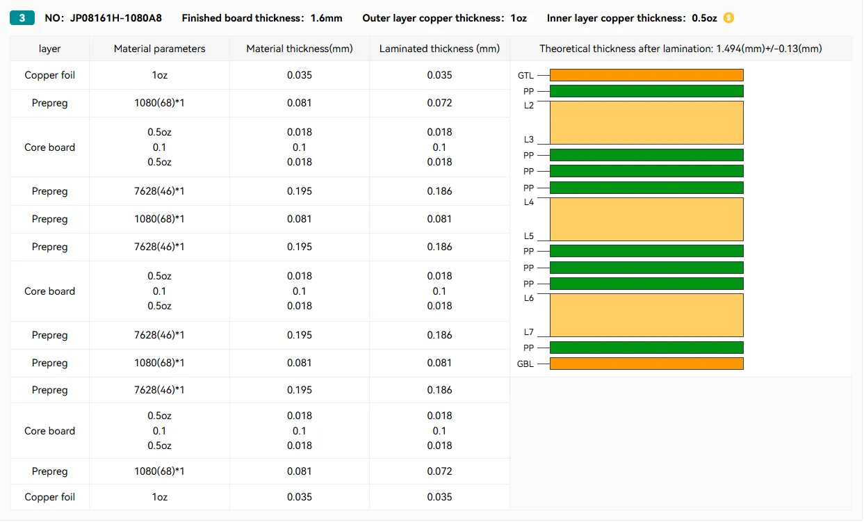
An 8-layer PCB consists of eight conductive copper layers separated by insulating dielectric materials, typically arranged in a symmetric stackup to minimize warpage and ensure mechanical stability. The layers alternate between signal routing, ground planes, and power distribution to support high-speed signals and controlled impedance. Factory processes involve multiple lamination cycles to bond these layers precisely, which distinguishes 8-layer boards from 4- or 6-layer alternatives. For electrical engineers, these boards matter because they handle complex circuits with dense interconnects, reducing electromagnetic interference through dedicated reference planes. In high-frequency applications, proper layer configuration prevents crosstalk and maintains signal integrity. Ultimately, opting for an 8-layer design balances performance demands against the elevated 8-layer PCB fabrication cost.
The relevance extends to production scalability, where initial prototypes reveal cost patterns that scale with volume. Engineers evaluate trade-offs between layer count and simpler routing on fewer layers to control expenses.
Core Factors Driving 8-Layer PCB Manufacturing Cost
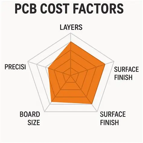
Several interconnected elements dictate the overall 8-layer PCB manufacturing cost. Board size directly impacts material usage and handling time, with larger panels requiring more resources during fabrication. Layer count introduces additional processing steps, such as repeated inner layer etching and alignment, which accumulate expenses. Material selection influences both raw costs and manufacturability, while feature density like via counts adds to drilling and plating demands. Production quantity plays a pivotal role, as setup costs amortize over higher volumes. Surface finishes and tolerances further modulate pricing based on durability requirements and inspection needs.
8-Layer PCB Material Cost: The Foundation of Pricing
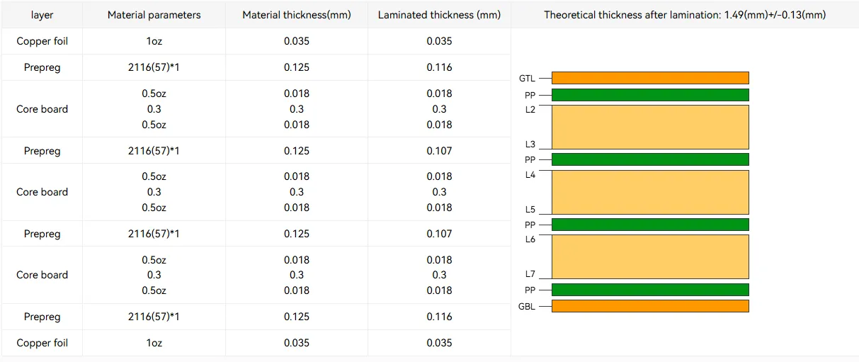
Materials form the baseline of 8-layer PCB material cost, with the core substrate like FR-4 providing dielectric separation between copper foils. Standard FR-4 suits most designs, but high-temperature variants become necessary for demanding thermal environments, elevating expenses due to specialized resin formulations. Copper foil thickness, often 1 oz per square foot on inner layers, adds weight and cost if heavier gauges are specified for current-carrying capacity. Prepreg sheets, used between cores during lamination, contribute significantly as their quantity scales with layer count. Factory insights reveal that material choices must align with performance specs to avoid rework. Optimizing stackup symmetry reduces material waste and warpage risks during pressing.
Solder mask and silkscreen layers add minimal cost but ensure protection and identification. Engineers should specify only essential thicknesses to keep 8-layer PCB material cost in check.
8-Layer PCB Fabrication Cost: Process-Intensive Steps
Fabrication dominates 8-layer PCB fabrication cost due to intricate sequential processes. Inner layer imaging and etching occur multiple times before lamination, requiring precise registration to prevent misalignment. Sequential lamination bonds cores and prepregs under high pressure and temperature, with 8 layers demanding at least three cycles for buildup. Drilling thousands of vias, including blind or buried types, consumes time and tooling, especially for small diameters under factory capabilities. Plating electroless copper and electroplating fill these vias, followed by outer layer processing and final profiling. Compliance with IPC-6012E standards ensures qualification through visual and electrical testing, adding to overhead but guaranteeing reliability.
Outer layer finishes like HASL provide cost-effective solderability, while alternatives like ENIG demand additional immersion steps. Routing complexity, such as fine-line traces below 4 mils, requires advanced exposure equipment. Panelization strategies help spread setup costs across multiple boards.
8-Layer PCB Assembly Cost: From Placement to Final Test
Assembly costs for 8-layer PCBs arise from component density and placement precision. Surface-mount technology dominates, with automated pick-and-place machines handling fine-pitch parts, but BGA or QFN packages necessitate underfill and X-ray inspection. Through-hole components add manual labor or selective soldering, increasing handling time. Solder paste printing uses stencils tailored to pad layouts, while reflow ovens profile temperatures for multilayer thermal mass. Conformal coating or potting protects against environments, incurring material and application fees. J-STD-001 guidelines dictate soldering quality, influencing test fixtures and functional verification.
Programming in-circuit tests and boundary scans verifies multilayer interconnects, with fixture costs scaling by pin count. Volume efficiencies reduce per-unit assembly rates through optimized line setups.
Achieving Cost-Effective 8-Layer PCB Design
Cost-effective 8-layer PCB design starts with stackup planning per IPC-2221B principles, prioritizing ground-power-signal symmetry to simplify impedance control. Minimize blind and buried vias by favoring through-hole where possible, reducing drilling expenses. Standardize trace widths and spacings to 5/5 mils unless high-speed demands tighter tolerances. Panelize designs efficiently for production runs, maximizing yield from standard panel sizes. Select economical surface finishes like HASL for non-critical pads to trim fabrication costs.
Collaborate early with fabricators on design for manufacturability, avoiding exotic features like embedded cavities. Simulate signal integrity upfront to validate layer allocation, preventing costly respins.
Use common via sizes above 8 mils to leverage standard tooling. Balance copper pour areas to prevent plating imbalances during fabrication.
Conclusion
Understanding the 8-layer PCB cost breakdown empowers electrical engineers to navigate trade-offs between performance and budget. Material selections set the foundation, while fabrication and assembly processes amplify expenses through complexity. By focusing on volume efficiencies and design optimizations, teams achieve reliable boards without excessive outlays. Factory-driven practices, aligned with key standards, ensure quality at each stage. Ultimately, proactive cost management turns 8-layer designs into viable solutions for demanding applications.
FAQs
Q1: What are the primary drivers of 8-layer PCB manufacturing cost?
A1: The main factors include layer count requiring multiple lamination cycles, board size affecting material use, via density increasing drilling time, and surface finish choices like ENIG over HASL. Material type, such as high-Tg FR-4, further elevates costs for thermal reliability. Production volume significantly lowers per-unit pricing through economies of scale. Engineers can mitigate by standardizing features and panelizing effectively.
Q2: How does 8-layer PCB material cost compare to simpler boards?
A2: 8-layer PCB material cost rises due to more prepreg sheets and cores for interlayer bonding, alongside potential high-performance dielectrics. Copper foil for eight layers adds proportionally, especially with heavier weights. Factory lamination demands precise material matching to avoid defects. Standard FR-4 keeps costs baseline, but upgrades for speed or heat push expenses higher. Optimization lies in symmetric stackups reducing waste.
Q3: What influences 8-layer PCB assembly cost the most?
A3: Component count and type dominate, with high-density BGAs requiring X-ray and rework capabilities. Multilayer thermal profiles extend reflow times, while testing verifies buried nets. J-STD-001 compliance adds inspection steps. SMT efficiencies scale with volume, but mixed THT increases labor. Design for testability with boundary scan cuts verification costs.
Q4: How can engineers achieve cost-effective 8-layer PCB design?
A4: Prioritize standard tolerances, minimize exotic vias, and follow IPC-2221B for stackup efficiency to streamline fabrication. Avoid over-specifying copper or finishes unless essential. Early DFM reviews prevent respins. High-volume quoting leverages panel yields. Balanced routing reduces impedance tuning needs, controlling overall 8-layer PCB fabrication cost.