ALLPCB


Are you struggling with a malfunctioning parking system due to issues with its printed circuit board (PCB)? Whether you're an engineer, technician, or facility manager, understanding how to diagnose and repair PCB problems in parking systems can save time and money. In this parking PCB troubleshooting guide, we’ll walk you through the steps to identify common PCB failures in parking systems, apply PCB repair techniques for parking systems, and use tools like a multimeter for multimeter testing parking PCB. Let’s dive into a detailed, step-by-step approach to diagnosing parking system faults and getting your system back up and running.
Introduction: Why Parking System PCBs Fail and How to Fix Them
Parking systems, whether for barriers, ticketing machines, or sensors, rely heavily on PCBs to manage operations like signal processing, power distribution, and communication between components. However, these circuit boards are prone to failures due to environmental factors, electrical stress, or manufacturing defects. A faulty PCB can cause issues like unresponsive barriers, incorrect ticket dispensing, or sensor malfunctions, disrupting parking operations.
This guide is designed to help you troubleshoot and repair PCBs in parking systems with practical tips and techniques. By following this parking PCB troubleshooting guide, you’ll learn how to spot common PCB failures in parking systems and apply effective solutions. We’ll also cover essential tools and methods, such as multimeter testing parking PCB, to ensure accurate diagnostics.
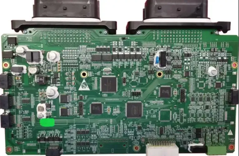
Understanding Parking System PCBs: What They Do
Before diving into troubleshooting, it’s important to understand the role of PCBs in parking systems. These boards act as the brain of the system, controlling functions like:
- Power management for motors and sensors.
- Signal processing for ticket readers or RFID scanners.
- Communication between the parking system and external devices like payment terminals.
PCBs in parking systems are often exposed to harsh conditions, including temperature fluctuations, humidity, and dust, which can lead to wear and tear over time. Recognizing the symptoms of a failing PCB is the first step in diagnosing parking system faults.
Common PCB Failures in Parking Systems
Identifying the root cause of a problem is crucial for effective troubleshooting. Below are some of the most common PCB failures in parking systems that you might encounter:
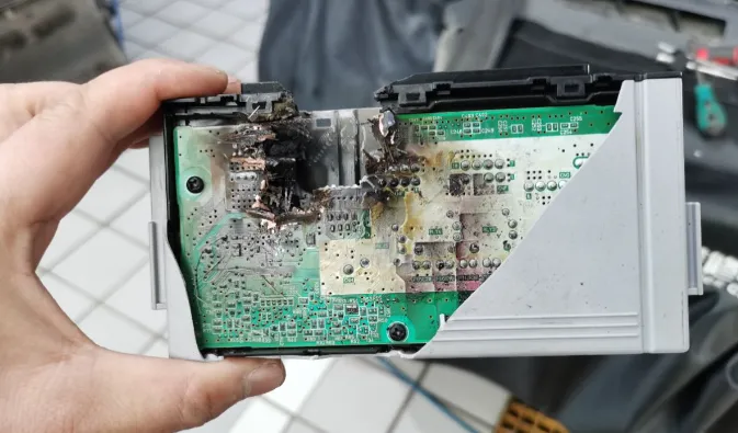
1. Component Burnout
Components like resistors, capacitors, and diodes on a PCB can burn out due to overvoltage or excessive heat. For instance, a capacitor rated for 16V might fail if exposed to a spike of 20V, leading to erratic system behavior or complete failure.
2. Solder Joint Cracks
Vibration and thermal expansion in parking systems can cause solder joints to crack, resulting in intermittent connections. This is common in outdoor parking barriers where temperature changes are frequent, often leading to issues like unresponsive controls.
3. Corrosion from Environmental Exposure
Moisture and dust can corrode PCB traces and components, especially in outdoor parking systems. Corrosion often appears as a greenish buildup on copper traces, disrupting electrical signals and causing failures in sensors or communication modules.
4. Power Supply Issues
Inconsistent or fluctuating power supply can damage sensitive components on the PCB. For example, a voltage drop below the required 12V for a parking barrier’s control board might prevent the motor from operating.
5. Signal Integrity Problems
Signal interference or degraded traces can disrupt communication between the PCB and other parts of the parking system. This often results in delayed responses or incorrect readings from sensors, with signal speeds dropping below optimal levels (e.g., from 1 MHz to erratic fluctuations).
Step-by-Step Parking PCB Troubleshooting Guide
Now that you’re familiar with common issues, let’s walk through a practical parking PCB troubleshooting guide to diagnose and fix faults. Follow these steps to systematically address problems in your parking system.
Step 1: Safety First
Before working on any PCB, disconnect the power supply to avoid electrical shocks. Ensure you’re working in a static-free environment by using an anti-static wrist strap to prevent damage to sensitive components.
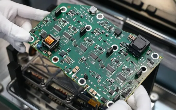
Step 2: Visual Inspection
Start by visually inspecting the PCB for obvious signs of damage. Look for:
- Burnt or bulging components (e.g., capacitors with a domed top).
- Cracked or broken solder joints.
- Corrosion or discoloration on traces and connectors.
A magnifying glass or a well-lit workspace can help you spot small defects. If you notice a burnt resistor, for instance, note its value (e.g., 220 ohms) for replacement.
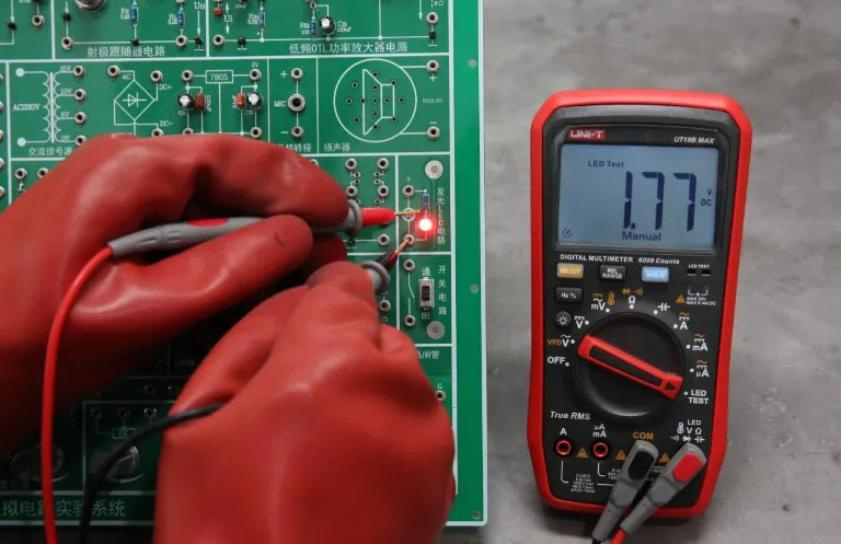
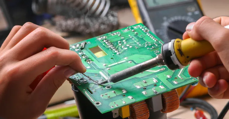
Step 3: Multimeter Testing Parking PCB
A multimeter is an essential tool for multimeter testing parking PCB. Use it to check for continuity, voltage, and resistance. Here’s how:
- Continuity Test: Set the multimeter to continuity mode and test PCB traces and solder joints. A beep indicates a good connection, while silence suggests a break.
- Voltage Test: Measure voltage at key points, such as power input pins. If the board requires 12V but you’re only reading 9V, there might be a power supply issue.
- Resistance Test: Check resistors and other components for correct values. A 1k ohm resistor reading significantly higher or lower indicates failure.
Step 4: Diagnosing Parking System Faults with Functional Testing
After basic checks, perform functional testing by reconnecting the PCB and observing the parking system’s behavior. For example, if a barrier doesn’t lift, trace the signal path from the control input to the motor driver on the PCB to identify where the signal stops.
Step 5: Isolate the Faulty Component
Once you’ve narrowed down the issue, isolate the faulty component or section of the PCB. If a specific capacitor near the power input shows no continuity, it’s likely the culprit behind power issues.
PCB Repair Techniques for Parking Systems
After diagnosing parking system faults, it’s time to apply PCB repair techniques for parking systems. Here are some common methods to fix issues:
1. Replacing Faulty Components
If a component like a capacitor or resistor is damaged, desolder it using a soldering iron and replace it with a new one of the same specifications. For instance, replace a 10uF, 25V capacitor with an identical part to ensure compatibility.
2. Repairing Solder Joints
For cracked solder joints, use a soldering iron and fresh solder to reconnect the joint. Apply flux to clean the area and ensure a strong bond. This is a common fix for intermittent issues in parking barrier control boards.
3. Cleaning Corrosion
If corrosion is present, gently clean the affected area with isopropyl alcohol and a soft brush. For severe corrosion, you may need to scrape away damaged traces and use a conductive pen to redraw the connection.
4. Addressing Power Issues
If power supply problems are detected, check external power sources and onboard voltage regulators. Replace any damaged regulators and ensure the input voltage matches the PCB’s requirements, such as a steady 12V for most parking system boards.
Preventing Future PCB Failures in Parking Systems
While troubleshooting and repairs are essential, preventing issues is just as important. Here are some tips to extend the life of your parking system PCBs:
- Protect from Environmental Damage: Use enclosures or conformal coatings to shield PCBs from moisture and dust, especially in outdoor systems.
- Ensure Stable Power Supply: Install surge protectors to prevent voltage spikes that can damage components.
- Regular Maintenance: Schedule periodic inspections to catch early signs of wear, such as loose connections or minor corrosion.
- Proper Installation: Avoid mechanical stress by securely mounting PCBs to prevent vibration-related damage.
Tools You’ll Need for Parking PCB Troubleshooting
Having the right tools makes parking PCB troubleshooting easier and more effective. Here’s a list of essentials:
- Multimeter: For voltage, continuity, and resistance testing.
- Soldering Iron and Solder: For replacing components and fixing joints.
- Desoldering Pump or Wick: To remove old solder during repairs.
- Magnifying Glass or Microscope: To inspect small components and traces.
- Isopropyl Alcohol and Brush: For cleaning corrosion and dirt.
- Anti-Static Wrist Strap: To protect sensitive components from static discharge.
When to Seek Professional Help
While many PCB issues can be fixed with the techniques above, some problems may require advanced skills or equipment. If the PCB has complex multilayer designs or if critical components like microcontrollers are damaged, consider consulting a professional repair service. This ensures the system is restored without risking further damage.
Conclusion: Mastering Parking System PCB Troubleshooting
Troubleshooting PCBs in parking systems doesn’t have to be overwhelming. By following this parking PCB troubleshooting guide, you can confidently diagnose and repair common PCB failures in parking systems. From visual inspections to multimeter testing parking PCB, and applying PCB repair techniques for parking systems, each step brings you closer to a fully functional system.
Regular maintenance and preventive measures can also minimize future issues, ensuring your parking system operates smoothly. Whether you’re dealing with a burnt component or a corroded trace, the methods outlined in this guide for diagnosing parking system faults will help you tackle challenges with ease. Keep your tools handy, stay patient, and you’ll master the art of PCB troubleshooting in no time.