 ALLPCB


If you're looking for the best PCB trace routing design rules to ensure manufacturability, you're in the right place. In a nutshell, effective PCB trace routing involves adhering to minimum width and spacing guidelines, optimizing trace paths for signal integrity, and considering manufacturing constraints like material limitations and fabrication tolerances. This blog dives deep into these principles, offering actionable advice on PCB trace minimum width, PCB trace minimum spacing, and other critical design rules to help you create reliable, high-performing circuit boards.
Introduction to PCB Trace Routing and Manufacturability
Printed Circuit Boards (PCBs) are the backbone of modern electronics, connecting components and ensuring devices function as intended. At the heart of PCB design lies trace routing—the process of laying out conductive paths that carry electrical signals between components. While this might seem straightforward, poor trace routing can lead to signal interference, manufacturing defects, and even complete board failure. That's why following PCB trace routing design rules is essential for manufacturability, ensuring your design can be produced efficiently and performs reliably.
In this comprehensive guide, we'll explore the best practices for PCB trace routing, focusing on key aspects like minimum trace width, minimum spacing, and other design considerations. Whether you're a seasoned engineer or just starting, these tips will help you design PCBs that meet industry standards and avoid costly production errors.

Why PCB Trace Routing Design Rules Matter
PCB trace routing isn't just about connecting points A to B. It's about ensuring that signals travel without interference, that the board can withstand manufacturing processes, and that it meets performance expectations. Poorly designed traces can result in issues like crosstalk, electromagnetic interference (EMI), or even short circuits. Additionally, if your design doesn't align with manufacturing capabilities, you might face delays or increased production costs.
By following established design rules, you can minimize these risks. These rules are often based on industry standards, such as those from the Institute of Printed Circuits (IPC), and are tailored to balance performance with manufacturability. Let's break down the core elements of PCB trace routing design rules, starting with the basics of trace width and spacing.
Understanding PCB Trace Minimum Width
One of the foundational elements of PCB trace routing design rules is determining the minimum trace width. Trace width refers to the thickness of the conductive path on the PCB, and it plays a critical role in both electrical performance and manufacturability.
Why Minimum Width Matters: If a trace is too narrow, it may not be able to carry the required current, leading to overheating or even trace burnout. On the other hand, excessively wide traces can waste valuable board space and complicate routing in dense designs. Additionally, manufacturing processes have limits—traces that are too thin may not be reliably produced due to etching inaccuracies.
General Guidelines for Minimum Trace Width: A common starting point for minimum trace width is 6 mils (0.006 inches) for standard designs, though this can vary based on the manufacturer and the specific requirements of your project. For high-current applications, trace widths might need to be 20 mils or more to handle the load without excessive heat buildup. The IPC-2221 standard provides detailed charts to calculate trace width based on current, temperature rise, and copper thickness (typically 1 oz/ft2 or 2 oz/ft2).
Practical Tip: Use online trace width calculators or design software with built-in tools to determine the appropriate width for your traces. Always check with your fabrication house for their specific minimum width capabilities—some may struggle with anything below 5 mils for standard processes.
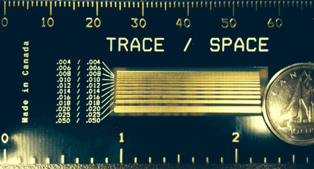
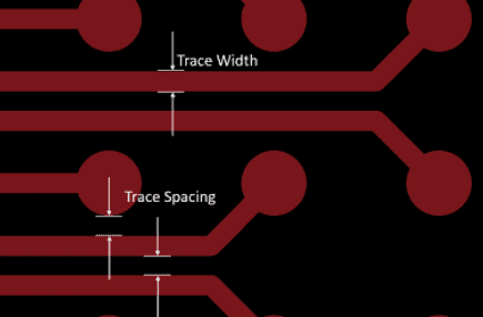
Mastering PCB Trace Minimum Spacing
Just as important as trace width is the spacing between traces, often referred to as PCB trace minimum spacing. This spacing ensures that traces don't interfere with each other electrically and that the board can be manufactured without defects like short circuits.
Why Minimum Spacing Matters: Insufficient spacing between traces can lead to crosstalk, where signals from one trace interfere with another, or even arcing in high-voltage designs. From a manufacturing perspective, inadequate spacing can result in copper bridges during etching, causing shorts.
General Guidelines for Minimum Spacing: A typical minimum spacing for low-voltage designs is 6 mils, though this increases for higher voltages to prevent breakdown. For example, at 50V, you might need at least 12 mils of spacing, while 500V could require over 100 mils, depending on the dielectric material and environmental factors. The IPC-2221 standard also provides detailed spacing requirements based on voltage and altitude (due to air breakdown risks).
Practical Tip: Always design with a safety margin beyond the minimum spacing requirements. If your manufacturer specifies a 6-mil minimum, aim for 8 mils where possible to account for fabrication tolerances. Additionally, consider the signal type—high-speed digital signals may require greater spacing or controlled impedance to prevent interference.
Key PCB Trace Routing Design Rules for Manufacturability
Beyond width and spacing, several other PCB trace routing design rules are critical for ensuring your board can be manufactured efficiently and performs as expected. Here are some of the most important practices to follow:
1. Optimize Trace Lengths for Signal Integrity
Long traces can introduce delays and signal degradation, especially in high-speed designs. For instance, in a design operating at 100 MHz, a trace longer than 1 inch might cause significant signal timing issues due to propagation delays (approximately 150 ps per inch on standard FR-4 material). Keep critical signal traces as short as possible, and use techniques like length matching for differential pairs to ensure signals arrive simultaneously.
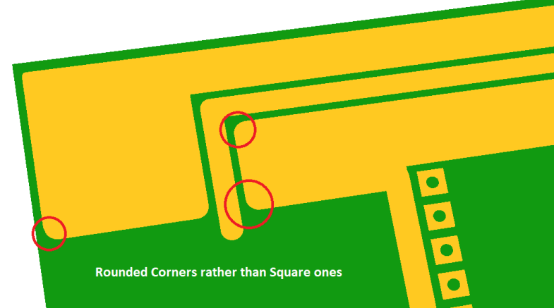
2. Avoid Sharp Corners in Trace Routing
Sharp 90-degree corners in traces can create signal reflection and EMI issues, especially in high-frequency designs. Instead, use 45-degree angles or smooth curves to maintain signal integ rity. From a manufacturing standpoint, sharp corners can also be more prone to etching errors, leading to uneven trace widths.
3. Consider Layer Stackup and Via Usage
In multilayer boards, trace routing often spans multiple layers, connected by vias. Minimize via usage to reduce manufacturing complexity and potential failure points. When vias are necessary, ensure they are placed away from high-current areas to avoid thermal stress. Additionally, work with your manufacturer to define a layer stackup that supports your trace routing needs while staying within cost constraints.
4. Account for Thermal Management
High-current traces generate heat, which can affect nearby components or the board itself if not managed properly. Use wider traces or copper pours for power and ground planes to dissipate heat effectively. For example, a trace carrying 5A might need a width of 50 mils on 1 oz copper to keep temperature rise below 10°C, per IPC guidelines.
5. Follow Design for Manufacturability (DFM) Guidelines
Always align your trace routing with the capabilities of your fabrication house. This includes adhering to their minimum trace width and spacing rules, avoiding overly complex routing that could increase production costs, and ensuring that your design files are formatted correctly for their processes. Many manufacturers provide DFM checklists—use them to validate your design before submission.
Advanced Tips for High-Speed and High-Density Designs
For more complex projects, such as those involving high-speed signals or densely packed components, additional PCB trace routing design rules come into play. Here are a few advanced considerations:
Controlled Impedance: High-speed signals, like those in USB or HDMI interfaces, often require specific trace impedance (e.g., 50 ohms for single-ended or 100 ohms for differential pairs). This is achieved by carefully calculating trace width, spacing, and the dielectric constant of the PCB material. Failing to maintain impedance can result in signal reflections and data loss.
Ground Planes: A solid ground plane beneath signal traces helps reduce EMI and provides a return path for signals. Avoid routing traces over splits in the ground plane, as this can introduce noise.
Differential Pair Routing: For differential signals, ensure traces are routed parallel to each other with consistent spacing to maintain signal integrity. Any mismatch in length or spacing can cause timing errors.
Common Mistakes to Avoid in PCB Trace Routing
Even with the best intentions, it's easy to make mistakes in PCB trace routing that can compromise manufacturability or performance. Here are some pitfalls to watch out for:
- Ignoring Manufacturer Specifications: Designing traces below the minimum width or spacing supported by your manufacturer can lead to production failures.
- Overloading Traces: Underestimating current requirements can cause traces to overheat, damaging the board.
- Poor Grounding: Inadequate ground planes or improper grounding can introduce noise and EMI, especially in high-speed designs.
- Neglecting Signal Integrity: Failing to account for trace length or impedance in high-speed designs can result in signal degradation.
Tools and Resources for Effective PCB Trace Routing
Designing PCBs with optimal trace routing doesn't have to be a manual process. Many software tools offer built-in features to help you adhere to design rules and validate your layout. These tools often include design rule checks (DRC) to flag issues like insufficient spacing or incorrect trace widths before you send your design for fabrication.
Additionally, leverage industry resources like the IPC standards (e.g., IPC-2221 for generic PCB design) to guide your routing decisions. Online communities and forums can also provide valuable insights from experienced designers facing similar challenges.
Conclusion: Building Better PCBs with Trace Routing Design Rules
Mastering PCB trace routing design rules is a critical step toward creating reliable, manufacturable circuit boards. By focusing on key factors like PCB trace minimum width and PCB trace minimum spacing, optimizing trace paths, and aligning your design with manufacturing capabilities, you can avoid common pitfalls and ensure your boards perform as intended.
Remember to start with the basics—adhere to minimum width and spacing guidelines based on current, voltage, and manufacturer limits. Then, refine your design by considering signal integrity, thermal management, and advanced techniques for high-speed or high-density layouts. With these best practices in mind, you'll be well-equipped to tackle any PCB design project with confidence.
At ALLPCB, we're committed to supporting your journey with resources and expertise to bring your designs to life. Follow these PCB trace routing design rules, and you'll be on your way to creating boards that meet both performance and manufacturability standards.


