 ALLPCB


Designing a power supply PCB layout is a critical step in ensuring the performance, reliability, and efficiency of electronic devices. A well-thought-out layout minimizes noise, reduces electromagnetic interference (EMI), and ensures stable power delivery. In this comprehensive guide, we’ll dive into the best placement and routing techniques for power supply PCB design, focusing on grounding, power planes, and other essential strategies. Whether you’re a beginner or an experienced engineer, this blog will provide actionable tips to optimize your PCB power supply layout.
Why Power Supply PCB Layout Matters
The layout of a power supply on a printed circuit board (PCB) directly impacts the stability and efficiency of the entire system. Poor placement or routing can lead to issues like voltage drops, excessive heat, and EMI, which can degrade performance or even cause system failures. By prioritizing a strategic PCB power supply layout, you can achieve low noise, better PCB thermal management, and improved signal integrity. Let’s explore the key techniques to master placement, routing, grounding, and the use of power planes in PCB design.
Key Principles of Power Supply PCB Layout
Before diving into specific techniques, it’s important to understand the core principles that guide power supply PCB design. These principles focus on minimizing interference, ensuring stable power delivery, and optimizing space.
- Minimize Loop Areas: Smaller loop areas in power and ground paths reduce inductance and EMI.
- Short and Direct Traces: Keep power traces as short and wide as possible to lower resistance and impedance, ideally maintaining a resistance below 0.01 ohms for high-current paths.
- Thermal Management: Place components to dissipate heat effectively and avoid hotspots.
- Signal Integrity: Separate high-current power paths from sensitive analog or digital signals to prevent crosstalk.
With these principles in mind, let’s break down the specific techniques for placement and routing in power supply PCB layouts.
Placement Techniques for Power Supply Components
Component placement is the foundation of a successful PCB power supply layout. Proper positioning reduces noise, improves efficiency, and simplifies routing. Here are the best practices for placing components.
1. Group Related Components
Place components that work together in close proximity to minimize trace lengths. For instance, position the input capacitors, inductors, and switching elements of a switching power supply near the power IC. This reduces parasitic inductance, which can otherwise cause voltage spikes. A typical guideline is to keep these components within 0.5 inches (12.7 mm) of the IC pins to maintain low impedance paths.
2. Position High-Current Components Strategically
Components like power MOSFETs, diodes, and inductors handle high currents and generate heat. Place them near the board’s edge or in areas with good airflow to aid heat dissipation. If using a heat sink, ensure there’s enough space around these components for proper mounting. Additionally, keep high-current paths away from sensitive analog circuits to avoid interference.
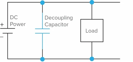
3. Place Decoupling Capacitors Close to ICs
Decoupling capacitors stabilize the voltage supply to ICs by filtering out noise. Position these capacitors as close as possible to the power pins of the IC, ideally within 0.1 inches (2.54 mm). Use short, direct traces or vias to connect them to the power and ground planes in PCB design. This ensures a low-inductance path, reducing noise in the power supply.
4. Optimize Input and Output Filter Placement
For power supplies, input and output filters (like capacitors and inductors) play a crucial role in smoothing voltage. Place input filters near the power input connector to block noise from entering the board. Similarly, position output filters close to the load to ensure clean power delivery. This setup helps maintain a stable voltage, often within ±5% of the target output.
Routing Techniques for Power Supply PCB Layout
Once components are placed, routing becomes the next critical step. Proper routing ensures efficient power delivery and minimizes interference. Here are the top routing strategies for a robust PCB power supply layout.
1. Use Wide Traces for High-Current Paths
Power traces carrying high currents need to be wide to handle the load without significant voltage drops or overheating. As a rule of thumb, use a trace width calculator to determine the appropriate size based on current and copper thickness. For example, a 1-ounce copper layer carrying 5A might require a trace width of at least 0.05 inches (1.27 mm) to keep temperature rise below 10°C.
2. Keep Power and Ground Traces Short
Long traces increase resistance and inductance, leading to voltage drops and noise. Route power and ground traces as directly as possible between components. If a trace must be longer, consider using a power plane in PCB design to provide a low-impedance path. This is especially important for high-frequency switching power supplies where even a small inductance can cause significant issues.
3. Avoid Crossing Sensitive Signals with Power Traces
High-current power traces can induce noise in nearby signal lines through electromagnetic coupling. Route power traces away from sensitive analog or digital signals. If crossing is unavoidable, ensure they intersect at a 90-degree angle to minimize coupling. Alternatively, use ground planes to shield sensitive signals from power traces.
Grounding Techniques for Power Supply PCB Layout
Grounding is one of the most critical aspects of a PCB power supply layout. A well-designed ground system reduces noise, prevents ground loops, and ensures safety. Let’s explore the best grounding practices.
1. Implement a Solid Ground Plane
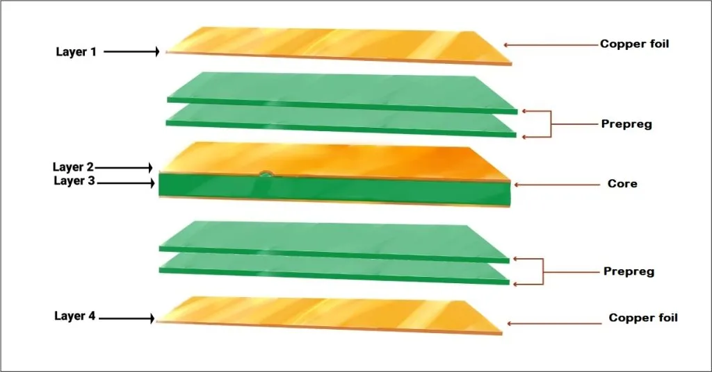
A ground plane is a large, continuous layer of copper dedicated to grounding. It provides a low-impedance return path for currents, reducing noise and EMI. For a 2-layer board, dedicate one layer primarily to ground. In a 4-layer board, use an inner layer as a ground plane to separate signal and power layers. Ensure the ground plane is unbroken under critical components like switching regulators to avoid impedance discontinuities.
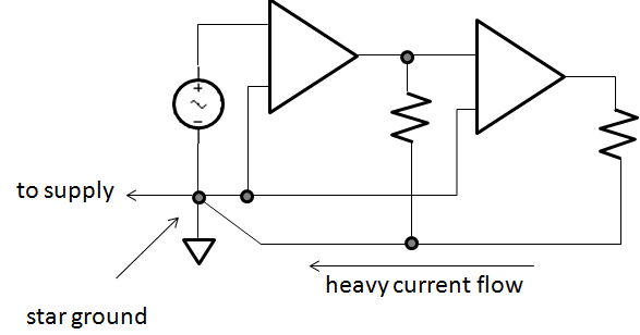
2. Use Star Grounding for Analog and Digital Circuits
In mixed-signal designs, separate analog and digital grounds to prevent noise from digital circuits affecting analog performance. Connect these grounds at a single point, often near the power supply input, using a star grounding technique. This minimizes ground loops and ensures clean power distribution. For example, in an audio amplifier PCB, the analog ground should not share a direct path with the noisy digital ground of a microcontroller.
3. Avoid Ground Loops
Ground loops occur when there are multiple return paths for current, leading to noise and interference. Design the ground plane to provide a single, direct return path for each circuit. If multiple ground paths are unavoidable, use ferrite beads or small resistors (e.g., 10 ohms) to isolate sections and break potential loops.
Power Planes in PCB Design: Best Practices
Power planes are dedicated copper layers used to distribute power across the PCB. They offer low impedance and high current-carrying capacity, making them ideal for power supply designs. Here’s how to use power planes effectively in PCB layouts.
1. Dedicate Layers for Power Planes
In multilayer boards (4 layers or more), assign one or more layers as power planes to distribute voltage levels like 3.3V or 5V. Place power planes adjacent to ground planes to create a low-inductance path for return currents. This setup also forms a natural capacitor between the planes, helping to filter high-frequency noise. For instance, a typical 4-layer stackup might be Signal-Ground-Power-Signal for optimal performance.
2. Split Power Planes for Multiple Voltages
If your design uses multiple voltage levels (e.g., 3.3V and 5V), split the power plane into separate regions for each voltage. Ensure clear boundaries between these regions to prevent cross-contamination of power domains. Use wide traces or copper pours to connect each region to its respective power source, maintaining at least 0.02 inches (0.5 mm) of separation between different voltage zones to avoid arcing.
3. Add Vias for Power Distribution
In multilayer designs, use vias to connect power planes to component pins on other layers. Place multiple vias for high-current connections to reduce resistance and improve reliability. For example, a power IC pin carrying 3A might need at least three 0.01-inch (0.25 mm) vias to ensure a low-impedance connection to the power plane.
Additional Tips for Optimizing Power Supply PCB Layout
Beyond placement, routing, grounding, and power planes, here are a few more tips to refine your PCB power supply layout for maximum performance.
- Simulate Your Design: Use simulation tools to analyze current flow, thermal performance, and EMI before manufacturing. This can help identify potential issues like voltage drops (targeting less than 0.1V for critical paths) or hotspots exceeding 50°C.
- Follow Manufacturer Guidelines: Power supply IC datasheets often include recommended layouts. Adhering to these can prevent common design errors and ensure optimal performance.
- Test for EMI Compliance: After layout completion, test the board for radiated and conducted emissions to ensure it meets standards like FCC or CE. Adding small filter components during testing can save redesign costs.
Common Mistakes to Avoid in Power Supply PCB Layout
Even with careful planning, certain mistakes can compromise a power supply PCB layout. Here are pitfalls to watch out for.
- Neglecting Ground Planes: Skipping a dedicated ground plane increases noise and EMI, especially in high-frequency designs.
- Overloading Traces: Undersized traces for high currents can overheat, potentially raising temperatures above safe limits like 85°C for standard FR-4 material.
- Ignoring Thermal Design: Placing heat-generating components too close together without proper dissipation can lead to thermal runaway.
Conclusion
A well-designed power supply PCB layout is essential for achieving reliable and efficient electronic systems. By focusing on strategic component placement, careful routing, robust grounding, and the use of power planes in PCB design, you can minimize noise, reduce EMI, and ensure stable power delivery. Remember to prioritize short traces, wide current paths, and solid ground planes while adhering to best practices for multilayer designs. With these techniques, your PCB power supply layout will support optimal performance, whether you’re working on a simple circuit or a complex high-power system.
At ALLPCB, we’re committed to helping engineers bring their designs to life with high-quality manufacturing and assembly services. Apply these placement and routing techniques to create robust power supply layouts, and trust us to support your next project with precision and care.


