 ALLPCB


In the fast-evolving world of electronics, small-batch PCB manufacturing with embedded components is becoming a game-changer for engineers and designers. If you're looking to create compact, high-performance circuit boards, embedding components directly into the PCB can save space, improve efficiency, and enhance reliability. But what exactly does this process involve, and how can it benefit your projects? In this detailed guide, we’ll walk you through the essentials of designing and manufacturing PCBs with integrated components, focusing on key concepts like buried components, components in cavities, and miniaturized PCB design.
Whether you're working on a prototype or a limited production run, understanding how to leverage embedded component technology can give your designs a competitive edge. Let’s dive into the details of this innovative approach and explore how it fits into small-batch PCB manufacturing.
What Are Embedded Components in PCBs?
Embedded components refer to electronic parts, such as resistors, capacitors, or even active devices like ICs, that are integrated directly into the layers of a printed circuit board (PCB) during the manufacturing process. Unlike traditional surface-mounted or through-hole components, these parts are either buried within the internal layers of the PCB or placed in specially designed cavities. This technique is often referred to as creating a "PCB with integrated components" or a "buried components PCB."
The primary goal of using embedded components is to reduce the overall size of the circuit board while improving electrical performance. By placing components inside the PCB, you eliminate the need for external connections, shorten trace lengths, and reduce parasitic inductance—issues that often affect high-speed designs. For instance, in a typical high-frequency application, shorter traces can lower signal loss, achieving impedance values as precise as 50 ohms for optimal signal integrity.
Why Choose Embedded Components for Small-Batch PCB Manufacturing?
Small-batch PCB manufacturing is ideal for prototyping, testing, and limited production runs, where flexibility and innovation are key. Incorporating embedded components into these batches offers several advantages, especially for projects requiring miniaturized PCB design. Here are some of the top benefits:
- Space Savings: Embedding components frees up valuable surface area on the PCB, allowing for more compact designs. This is critical in industries like wearables or medical devices, where size constraints are strict. For example, a smartwatch PCB might reduce its footprint by 30% using embedded capacitors and resistors.
- Improved Performance: Shorter interconnects between components reduce signal delays and interference. In high-speed circuits, this can improve signal speeds by up to 20%, ensuring better performance for applications like 5G modules.
- Enhanced Reliability: With fewer exposed solder joints, the risk of mechanical failure or environmental damage (like moisture ingress) is minimized. This is particularly useful in harsh environments, such as aerospace or automotive applications.
- Cost-Effectiveness in Small Runs: While embedding components can increase initial design complexity, it reduces assembly steps in small-batch production, potentially lowering costs for limited runs by streamlining the process.
For engineers working on niche or experimental projects, these benefits make embedded component PCBs a powerful choice for achieving cutting-edge designs without sacrificing quality.
Types of Embedded Component Technologies
When designing a PCB with integrated components, there are several approaches to embedding parts. Understanding these methods can help you choose the right technique for your project. Below, we explore the most common types:
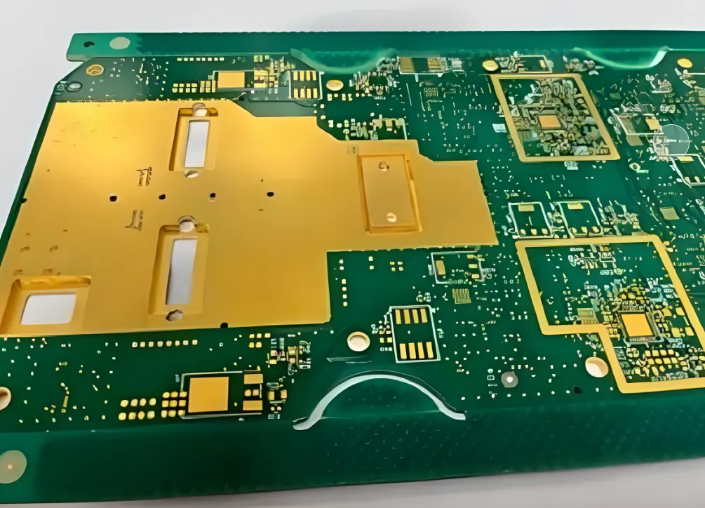
1. Buried Components PCB
In a buried components PCB, parts are placed within the inner layers of the board during the lamination process. These components are completely enclosed by the PCB material, protecting them from external factors and reducing the board’s surface clutter. This method is ideal for passive components like resistors and capacitors, which don’t require frequent replacement or access.
For example, in a multilayer PCB with 8 layers, a designer might embed a 10kΩ resistor between layers 3 and 4, connecting it via microvias to minimize trace length. This setup can reduce parasitic effects by as much as 15% compared to surface-mounted alternatives.
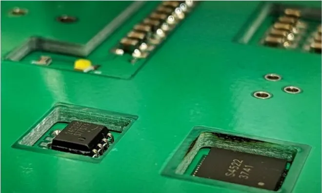
2. Component in Cavity PCB
Another approach is the component in cavity PCB, where a recessed area or cavity is created within the board to house a specific component. This method is often used for larger or active components, like microcontrollers or power modules, which may need occasional access or heat dissipation. The cavity protects the component while keeping the board’s profile slim.
In a practical scenario, a cavity might be designed to hold a 3mm x 3mm IC, with thermal vias integrated to manage heat dissipation, ensuring the component operates within a safe temperature range of 85°C or below.
3. Fully Integrated Components
Fully integrated components are embedded during the PCB fabrication process using advanced techniques, such as forming resistors or capacitors directly from the board’s materials (like copper and dielectric layers). This method is less common in small-batch manufacturing due to higher setup costs but offers unparalleled miniaturization for high-density designs.
Design Considerations for Miniaturized PCB Design with Embedded Components
Creating a miniaturized PCB design with embedded components requires careful planning and attention to detail. While the benefits are clear, the design process can be more complex than traditional PCB layouts. Here are some critical factors to consider:
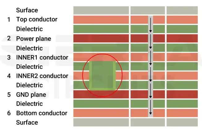
1. Layer Stack-Up Planning
The PCB’s layer stack-up must be designed to accommodate embedded components without compromising structural integrity. For instance, placing a capacitor between layers 2 and 3 in a 6-layer board requires precise alignment of vias and traces to ensure connectivity. Misalignment can lead to signal integrity issues or manufacturing defects.
2. Thermal Management
Embedded components can generate heat within the PCB, especially active devices like ICs. Without proper thermal vias or heat sinks, temperatures can rise, affecting performance. Designers often use simulation tools to predict heat distribution and ensure the board stays within safe limits, typically below 100°C for most components.
3. Component Selection
Not all components are suitable for embedding. Choose parts that are rated for the embedding process, as they must withstand the heat and pressure of lamination (often around 180°C and 300 psi). Thin, low-profile components are preferred to avoid increasing the board’s thickness.
4. Signal Integrity and Routing
Embedding components allows for shorter trace lengths, but routing must still be optimized to avoid crosstalk or interference. For high-speed designs, maintaining controlled impedance (e.g., 50 ohms for RF signals) is critical. Use design software to simulate signal paths and adjust layouts accordingly.
The Manufacturing Process for Embedded Component PCBs
Manufacturing PCBs with embedded components in small batches involves several specialized steps. While the exact process may vary depending on the design and technology used, here’s a general overview of how it works:
- Design and Simulation: Engineers create a detailed layout using CAD software, specifying the placement of embedded components and running simulations to verify performance. This step often includes thermal and electrical analysis to prevent issues during production.
- Material Selection: High-quality laminates and prepregs are chosen to ensure the PCB can withstand the embedding process. Materials with low dielectric constants (e.g., 3.5 or below) are often used for high-frequency applications.
- Component Placement: Components are placed in cavities or between layers during the board’s assembly. For buried components, this happens before lamination, while cavity components may be inserted after partial fabrication.
- Lamination and Pressing: The PCB layers are stacked and pressed under high heat and pressure to bond them together, encapsulating the embedded components. This step requires precise control to avoid damaging delicate parts.
- Drilling and Via Formation: Microvias or blind vias are drilled to connect embedded components to other layers. Laser drilling is often used for precision, creating vias as small as 0.1mm in diameter.
- Testing and Validation: After manufacturing, the PCB undergoes rigorous testing to check for electrical continuity, signal integrity, and thermal performance. This ensures the embedded components function as intended.
For small-batch runs, manufacturers often use advanced equipment to maintain precision, even with low volumes. This allows engineers to test innovative designs without committing to large-scale production.
Applications of Embedded Component PCBs in Small-Batch Projects
The use of embedded component PCBs is growing across various industries, especially in small-batch manufacturing where customization and performance are priorities. Here are some common applications:
- Wearable Electronics: Devices like fitness trackers and smartwatches rely on miniaturized PCB designs to fit complex circuitry into tiny spaces. Embedding components reduces size while maintaining functionality.
- Medical Devices: Portable diagnostic tools and implantable devices benefit from the reliability and compactness of embedded component PCBs. For example, a hearing aid might use buried capacitors to save space and improve battery life.
- Aerospace and Defense: High-reliability applications in harsh environments use embedded components to reduce failure points and protect sensitive electronics from vibration or temperature extremes.
- IoT Devices: Internet of Things (IoT) products often require small, efficient PCBs to connect sensors and communication modules. Embedded components help achieve this while keeping costs manageable for small runs.
Challenges and Solutions in Small-Batch Embedded Component PCB Manufacturing
While the benefits are significant, there are challenges to consider when incorporating embedded components into small-batch PCB manufacturing. Here’s a look at common issues and how to address them:
Challenge 1: Higher Initial Design Costs
Designing a PCB with integrated components requires advanced software and expertise, which can increase upfront costs, especially for small runs. However, this can be offset by reduced assembly costs and improved performance, making it a worthwhile investment for high-value projects.
Challenge 2: Manufacturing Complexity
Embedding components adds steps to the fabrication process, requiring specialized equipment and tight tolerances. Partnering with an experienced manufacturer can help ensure precision and minimize defects, even in low-volume production.
Challenge 3: Limited Component Access
Once embedded, components are difficult to replace or repair. To mitigate this, use simulation tools during the design phase to validate performance and choose reliable, high-quality parts to reduce the likelihood of failure.
How to Get Started with Embedded Component PCBs
If you’re ready to explore embedded component PCBs for your next small-batch project, here are some practical steps to begin:
- Define Your Requirements: Determine the specific components to embed and the performance goals for your design, such as size reduction or signal speed improvements.
- Choose the Right Tools: Use advanced PCB design software that supports embedded component layouts and simulations to optimize your design before manufacturing.
- Collaborate with Experts: Work closely with your manufacturing partner to ensure they have the capabilities to handle embedded component technology, even for small batches.
- Start with a Prototype: Test your design with a small run to identify any issues before scaling up. This approach minimizes risk and allows for adjustments.
Conclusion: The Future of Small-Batch PCB Manufacturing with Embedded Components
Small-batch PCB manufacturing with embedded components offers a powerful solution for engineers and designers aiming to push the boundaries of innovation. By integrating components directly into the board—whether through buried components, cavities, or other techniques—you can achieve miniaturized PCB designs that deliver superior performance and reliability. From wearables to aerospace applications, the potential of this technology is vast, especially for niche or experimental projects.
As manufacturing processes continue to evolve, the barriers to adopting embedded component PCBs in small batches are decreasing. With careful planning and the right partnerships, you can leverage this approach to create cutting-edge electronics that stand out in today’s competitive market. Whether you’re focused on reducing size, enhancing efficiency, or improving durability, embedded component PCBs are a step toward the future of electronics design.


