 ALLPCB


Are you looking to design a high-power circuit board that can handle significant current without overheating or failing? If so, 3 oz copper PCBs might be your solution. These heavy copper boards are ideal for high current applications, offering greater current capacity and improved thermal management compared to standard 1 oz or 2 oz copper PCBs. In this guide, we’ll dive deep into the specifics of 3 oz copper PCB current capacity, explore tools like a 3 oz copper PCB trace width calculator, and provide actionable tips on high current PCB design, PCB thermal management techniques, and PCB power layer design. Let’s unlock the power of 3 oz copper PCBs together!
Why Choose 3 oz Copper PCBs for High-Power Designs?
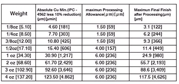
For electrical engineers working on power electronics, automotive systems, or industrial equipment, the demand for robust circuit boards is ever-growing. A 3 oz copper PCB refers to a board with a copper thickness of 3 ounces per square foot, which translates to about 4.2 mils (0.0042 inches) of copper thickness. This is significantly thicker than the standard 1 oz copper (1.4 mils), making it a go-to choice for applications requiring high current capacity and better heat dissipation.
The primary advantage of 3 oz copper is its ability to carry more current without excessive temperature rise. For instance, while a 1 oz copper trace might handle around 1-2 amps for a 10-mil-wide trace at a 10°C temperature rise, a 3 oz copper trace of the same width can handle approximately 3-5 amps under similar conditions, depending on the design and ambient temperature. This makes it ideal for power supplies, motor controllers, and other high-current applications.
Understanding 3 oz Copper PCB Current Capacity
One of the most critical aspects of designing with 3 oz copper PCBs is understanding their current capacity. The current-carrying capacity of a PCB trace depends on several factors: trace width, copper thickness, temperature rise, and ambient conditions. For 3 oz copper, the increased thickness means a larger cross-sectional area, which directly correlates to higher current capacity.
According to industry standards like IPC-2221, the current capacity for a 3 oz copper trace can be significantly higher than thinner copper layers. For example, a 50-mil-wide trace with 3 oz copper can handle upwards of 10-15 amps with a 10°C temperature rise in an external layer, assuming standard ambient conditions (25°C). This is roughly three times the capacity of a 1 oz copper trace of the same width under identical conditions.
However, it’s not just about raw numbers. Engineers must account for real-world factors like trace length, board stackup, and whether the trace is on an internal or external layer. Internal layers, due to less airflow, have lower current capacities—often 50-60% less than external traces. This is why proper design and simulation tools are essential for accurate predictions.
Using a 3 oz Copper PCB Trace Width Calculator
Calculating the right trace width for your 3 oz copper PCB is crucial to ensure safety and performance. A 3 oz copper PCB trace width calculator simplifies this process by allowing you to input parameters like desired current, copper thickness, temperature rise, and layer type to determine the minimum trace width required.
For instance, using a tool like the one provided by DigiKey or Sierra Circuits, let’s say you need to carry 12 amps on an external 3 oz copper layer with a maximum temperature rise of 20°C. The calculator might suggest a trace width of approximately 60 mils (1.5 mm). These tools often base their calculations on IPC-2221 standards, ensuring reliable results for most applications.
Here’s a quick step-by-step guide to using a trace width calculator:
- Enter the desired current (e.g., 12 amps).
- Select the copper thickness (3 oz or 105 μm).
- Specify the maximum allowable temperature rise (e.g., 10°C or 20°C).
- Choose the layer type (internal or external).
- Review the recommended trace width and adjust your design accordingly.
These calculators are invaluable for engineers, saving time and reducing the risk of design errors. Many are available online for free, and I recommend testing a few to cross-verify results for critical projects.
Key Principles of High Current PCB Design
Designing for high current goes beyond just selecting 3 oz copper. High current PCB design requires a holistic approach to ensure reliability and longevity. Here are some key principles to follow:
1. Optimize Trace Width and Spacing
As discussed, wider traces carry more current, but spacing is equally important to prevent arcing or crosstalk in high-voltage designs. For 3 oz copper carrying 10+ amps, maintain at least 20-30 mils of spacing between traces to avoid issues, especially at voltages above 50V.
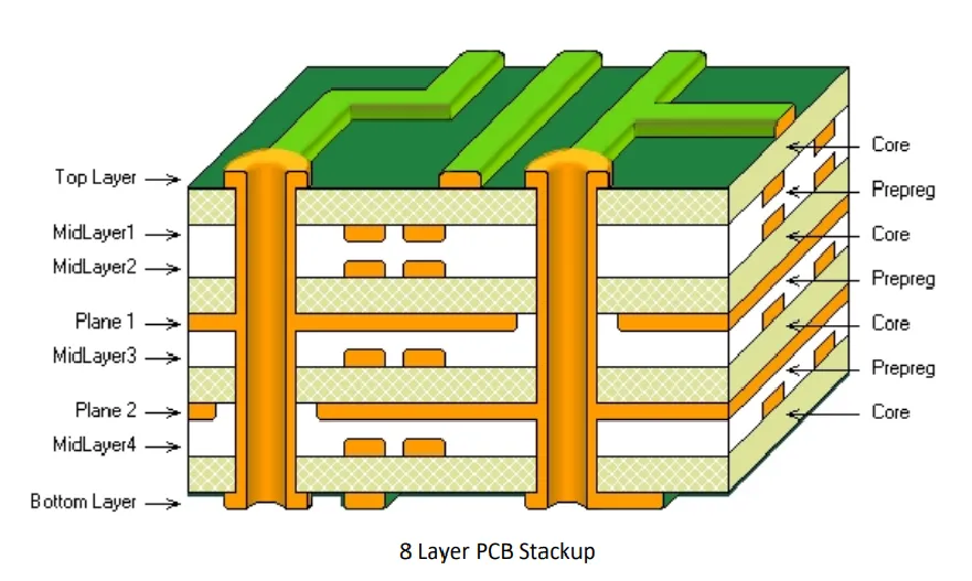
2. Use Multiple Layers for Power Distribution
In high-current designs, a single trace might not be enough. Distribute current across multiple layers or use power planes to reduce resistance and heat buildup. For example, a 4-layer board with dedicated power and ground planes can handle significantly more current than a 2-layer board.
3. Minimize Trace Length
Long traces increase resistance, leading to voltage drops and heat generation. Keep power traces as short as possible, and use vias strategically to connect layers without introducing excessive resistance.
4. Reinforce with Copper Fills and Vias
For very high currents, consider using copper fills or “pours” to increase the effective cross-sectional area. Additionally, stitch power planes with multiple vias to ensure even current distribution and reduce thermal hotspots.
PCB Thermal Management Techniques for 3 oz Copper Designs
Heat is the enemy of high-current designs. Without proper PCB thermal management techniques, even a 3 oz copper PCB can fail due to overheating. Here are proven strategies to keep temperatures in check:
1. Leverage Copper Thickness for Heat Dissipation
The thicker copper in a 3 oz PCB naturally conducts heat better than thinner layers. Use this to your advantage by designing wide traces and large copper areas to act as heat sinks, spreading thermal energy across the board.
2. Add Thermal Vias
Thermal vias are small holes filled or plated with copper that transfer heat from one side of the board to the other. Place them near high-power components or under ICs to channel heat to a ground plane or external heat sink. For a 3 oz copper board, a grid of 10-15 thermal vias under a power component can reduce temperature by 5-10°C.
3. Use Heat Sinks and Fans
For applications pushing the limits of 3 oz copper (e.g., currents above 20 amps), external cooling solutions like heat sinks or fans may be necessary. Attach heat sinks directly to large copper areas for maximum effect, ensuring thermal paste is used for good contact.
4. Optimize Component Placement
Place high-power components away from each other to avoid concentrated heat zones. Also, position them near board edges or areas with good airflow to enhance natural cooling.
Mastering PCB Power Layer Design with 3 oz Copper
A well-designed power layer is the backbone of any high-current PCB. PCB power layer design with 3 oz copper involves creating dedicated planes for power and ground to minimize impedance and ensure stable voltage delivery. Here’s how to do it right:
1. Dedicate Layers to Power and Ground
In a multilayer PCB (4 layers or more), assign entire layers to power and ground. For instance, in a 4-layer stackup, use Layer 2 as a ground plane and Layer 3 as a power plane. With 3 oz copper, these planes can handle substantial current—often 20-30 amps or more across the plane—without significant voltage drop.
2. Minimize Loop Inductance
Place power and ground planes adjacent to each other to reduce loop inductance, which can cause noise and voltage spikes in high-current designs. The closer the planes, the better the decoupling effect.
3. Use Decoupling Capacitors
Place decoupling capacitors near power pins of ICs to filter noise and stabilize voltage. For high-current designs, use a mix of ceramic and electrolytic capacitors (e.g., 0.1 μF and 10 μF) to cover a range of frequencies.
4. Split Power Planes if Needed
For boards with multiple voltage levels (e.g., 5V and 12V), split the power plane into sections. Ensure each section has enough 3 oz copper area to handle the current for that voltage domain, and use ferrite beads or inductors to isolate noise between sections.
Practical Tips and Common Pitfalls to Avoid
Designing with 3 oz copper PCBs comes with unique challenges. Here are some practical tips based on real-world experience, along with pitfalls to avoid:
- Tip: Always simulate your design using tools like Altium Designer or KiCad with thermal and current density analysis plugins. This helps identify hotspots before fabrication.
- Pitfall: Don’t assume 3 oz copper solves all thermal issues. Without proper airflow or cooling, even thick copper can overheat under sustained high current.
- Tip: Work closely with your PCB manufacturer to confirm 3 oz copper availability and any design rule constraints, as not all fabricators handle heavy copper easily.
- Pitfall: Avoid over-relying on vias for current carrying. While vias help, too many in a small area can weaken the board structurally.
Conclusion: Harness the Full Potential of 3 oz Copper PCBs
Designing with 3 oz copper PCBs opens up new possibilities for high-power applications, offering unmatched 3 oz copper PCB current capacity and thermal performance. By using tools like a 3 oz copper PCB trace width calculator, adhering to high current PCB design best practices, implementing effective PCB thermal management techniques, and optimizing PCB power layer design, you can create reliable, efficient boards for even the most demanding projects.
Whether you’re working on a power supply for industrial equipment or a motor controller for electric vehicles, the principles outlined in this guide will help you succeed. Start by calculating your trace widths, simulate your designs, and always prioritize thermal management.


