ALLPCB


For electrical engineers working on high-speed PCB design, one critical question often arises: How does inner layer copper thickness affect signal integrity? In short, copper thickness in the inner layers of a printed circuit board (PCB) directly influences impedance values, signal loss, and overall performance, especially in high-speed applications. Thicker copper can reduce resistive losses but may complicate impedance control, while thinner copper offers better precision for fine traces but increases signal loss at high frequencies. This blog dives deep into the nuances of inner layer copper thickness, exploring its effects on PCB signal integrity, impedance, and signal loss reduction, with practical insights for optimizing your designs.
Why Inner Layer Copper Thickness Matters in PCB Design
In the world of high-speed PCB design, every detail counts. As data rates climb beyond 10 GHz in applications like 5G, AI chips, and high-performance computing, maintaining signal integrity becomes a top priority. Signal integrity refers to the ability of a signal to travel through a PCB without distortion, interference, or loss. Inner layer copper thickness plays a pivotal role here, affecting how signals propagate through the board.
Copper thickness impacts several key factors:
- Impedance Control: The thickness of copper affects the characteristic impedance of transmission lines, which must be matched to prevent reflections.
- Signal Loss: Thicker copper reduces resistive losses, especially at high frequencies where the skin effect dominates.
- Thermal Management: Thicker layers can handle more current and dissipate heat better, reducing risks of overheating in power planes.
Understanding these effects is essential for engineers designing PCBs for high-speed applications. Let’s break down each aspect to see how inner layer copper thickness influences performance and what you can do to optimize your designs.
Inner Layer Copper Thickness and PCB Signal Integrity
Signal integrity is the cornerstone of reliable PCB performance. When signals degrade due to noise, crosstalk, or loss, the entire system can fail. Inner layer copper thickness directly affects signal integrity by influencing how signals travel through embedded traces.
In high-speed designs, signals often travel through striplines—traces sandwiched between two ground planes in the inner layers. The copper thickness of these traces and the surrounding planes impacts the electromagnetic field distribution. For instance, a typical copper thickness of 1 oz (35 μm) might work well for standard designs, but for high-speed applications operating at 25 Gbps or higher, engineers often opt for 0.5 oz (17 μm) copper to achieve finer trace widths and better impedance control.
However, thinner copper increases resistance, leading to higher signal loss. At 10 GHz, the skin effect—where current flows primarily on the surface of the conductor—becomes significant. A thinner copper layer means less effective conductive area, increasing attenuation. Balancing thickness with signal integrity needs is a delicate act. Engineers often use simulation tools like Ansys HFSS or Altium Designer to model these effects and find the sweet spot for their specific application.
Key Takeaway for Signal Integrity
For optimal PCB signal integrity, consider the frequency range of your design. If you’re working with frequencies above 5 GHz, thinner copper (0.5 oz) might be necessary for precise impedance matching, but be prepared to address higher losses with better materials or shorter trace lengths. For lower frequencies, thicker copper (1-2 oz) can reduce losses and improve robustness.
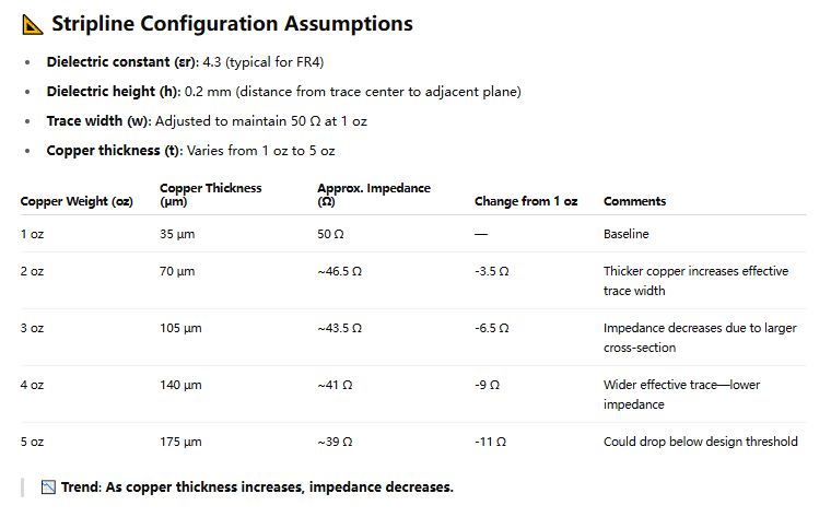
The Copper Thickness Effect on Inner Layer Impedance
Impedance control is a critical factor in high-speed PCB design. Mismatched impedance causes signal reflections, leading to data errors and reduced performance. The characteristic impedance of a trace depends on several factors, including trace width, dielectric thickness, and copper thickness in the inner layers.
Thicker copper reduces the impedance of a trace because it increases the cross-sectional area of the conductor. For example, a stripline with 1 oz copper might have a characteristic impedance of 50 ohms with a specific trace width and dielectric height. If you increase the copper thickness to 2 oz (70 μm), the impedance could drop to 48 ohms unless you adjust the trace width or dielectric spacing. This shift might seem small, but even a 2-ohm mismatch can cause significant reflections at high frequencies.
Conversely, thinner copper increases impedance, which can be beneficial for achieving higher impedance values (like 75 ohms) in compact designs. However, it requires tighter manufacturing tolerances, as small variations in thickness can lead to larger impedance deviations. PCB manufacturers often specify a tolerance of ±10% for copper thickness, which can translate to impedance variations of ±1-2 ohms—enough to disrupt high-speed signals if not accounted for.
Practical Tip for Impedance Control
Use PCB stackup calculators or simulation software to predict impedance based on copper thickness. Collaborate with your PCB manufacturer to ensure tight control over copper deposition processes. For critical designs, request impedance testing on prototypes to verify values before full production.
Signal Loss Reduction: Finding the Right Copper Thickness
Signal loss is a major concern in high-speed PCB design, especially as frequencies increase. Losses come in two main forms: conductor loss (due to resistance in the copper) and dielectric loss (due to the insulating material). Inner layer copper thickness primarily affects conductor loss.
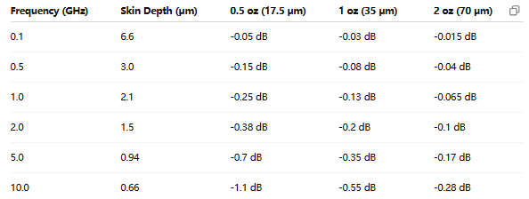
At high frequencies, the skin effect causes current to flow near the surface of the conductor, reducing the effective cross-sectional area. For a 1 oz copper layer at 1 GHz, the skin depth is approximately 2.1 μm, meaning most of the current flows within this thin layer. If the copper is only 17 μm thick (0.5 oz), the loss is higher compared to a 35 μm (1 oz) layer because there’s less material for the current to spread across beyond the skin depth.
However, thicker copper isn’t always better. Beyond a certain point—typically 2 oz for most high-speed applications—increasing thickness offers diminishing returns because the skin effect limits how much of the additional copper is used. Plus, thicker copper can make etching more difficult, leading to less precise trace geometries and potential impedance mismatches.
Strategies for Signal Loss Reduction
To minimize signal loss while optimizing copper thickness:
- Choose a copper thickness based on your frequency range. For 1-5 GHz, 1 oz copper often strikes a good balance. For 10 GHz and above, consider 0.5 oz with low-loss dielectrics like Rogers RO4000 series.
- Use smoother copper finishes to reduce surface roughness, which exacerbates skin effect losses. As noted in recent industry discussions, copper roughness can increase losses by up to 20% at high frequencies.
- Keep trace lengths as short as possible to limit the cumulative effect of conductor loss.
High-Speed PCB Design: Balancing Copper Thickness with Other Factors
In high-speed PCB design, copper thickness is just one piece of the puzzle. Engineers must balance it with other factors like dielectric material, trace width, and layer stackup. For instance, using a low dielectric constant (Dk) material like PTFE can reduce signal delay and loss, complementing the benefits of optimized copper thickness.
Consider a real-world example: designing a PCB for a 25 Gbps data link. The engineer might select a stackup with 0.5 oz inner layer copper to achieve precise 50-ohm impedance with narrow traces. However, to counteract the higher resistive loss, they pair it with a low-loss dielectric (Dk of 3.0) and minimize trace length by optimizing component placement. Simulations show that this combination keeps insertion loss below 1 dB over a 10-inch trace at 12.5 GHz (half the data rate frequency).
Collaboration with your PCB fabricator is crucial here. They can advise on achievable copper thicknesses and tolerances for your design. Some manufacturers offer hybrid stackups, combining thicker copper for power planes and thinner copper for signal layers, providing the best of both worlds.
Practical Considerations for Choosing Copper Thickness
Selecting the right inner layer copper thickness isn’t just about theory—it’s about practical constraints too. Here are some actionable tips for electrical engineers:
- Application Requirements: Determine the frequency, data rate, and power needs of your design. High-speed digital signals often need thinner copper for precision, while power delivery might require thicker layers (2 oz or more).
- Manufacturing Limits: Check with your PCB supplier on available copper thicknesses. Standard options are 0.5 oz, 1 oz, and 2 oz, but custom thicknesses may increase cost and lead time.
- Cost vs. Performance: Thicker copper and tighter tolerances raise fabrication costs. Weigh these against performance gains. For non-critical designs, 1 oz copper often suffices.
- Thermal and Current Capacity: Thicker copper handles higher currents and dissipates heat better. Use IPC-2221 calculators to ensure your copper thickness meets current-carrying requirements.
Common Pitfalls to Avoid with Inner Layer Copper Thickness
Even experienced engineers can stumble when dealing with copper thickness in PCB design. Here are some common mistakes to watch out for:
- Ignoring Skin Effect: Failing to account for skin effect at high frequencies can lead to unexpected signal loss. Always consider frequency when choosing thickness.
- Overlooking Tolerance: Assuming copper thickness is exact can cause impedance mismatches. Factor in manufacturing tolerances (typically ±10%) during design.
- Neglecting Stackup Symmetry: Uneven copper thicknesses across layers can cause warpage during fabrication. Aim for a balanced stackup to maintain board flatness.
Conclusion: Optimizing Inner Layer Copper Thickness for Signal Integrity
Inner layer copper thickness is a critical factor in unlocking the full potential of your PCB, especially in high-speed designs. It directly impacts PCB signal integrity, inner layer impedance, and signal loss reduction. By carefully selecting copper thickness—whether 0.5 oz for precision or 1-2 oz for reduced loss—you can tailor your design to meet specific performance goals. Remember to balance thickness with other factors like dielectric choice, trace geometry, and manufacturing constraints.
As an electrical engineer, your goal is to create reliable, high-performing PCBs. Use simulation tools, collaborate with fabricators, and test prototypes to ensure your copper thickness choice aligns with your application’s needs.