 ALLPCB


Are you looking to push the boundaries of electronic design with innovative, space-saving solutions? Flexible PCBs (Printed Circuit Boards) are the answer. They offer unparalleled design freedom, allowing engineers to create compact, lightweight, and durable circuits for a wide range of applications. In this comprehensive guide, we’ll explore flexible PCB design rules, bending radius considerations, materials selection, and stackup configurations to help you harness their full potential. Whether you’re designing for wearables, medical devices, or aerospace systems, this post will equip you with the knowledge to succeed.
What Are Flexible PCBs and Why Do They Matter?
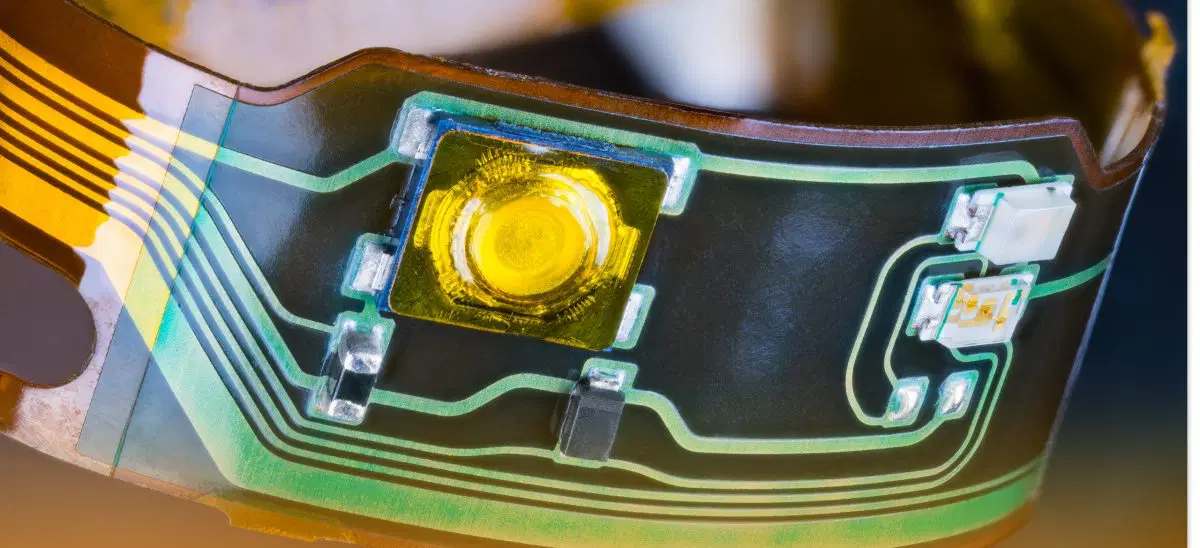
Flexible PCBs are thin, lightweight circuit boards made from flexible materials that can bend, fold, or twist without breaking. Unlike traditional rigid PCBs, they adapt to unique shapes and fit into tight spaces, making them ideal for modern electronics where size and weight are critical. From smartphones to automotive sensors, flexible PCBs are revolutionizing industries by enabling smaller, more efficient designs.
The importance of flexible PCBs lies in their ability to reduce assembly costs, improve reliability, and support dynamic applications. By understanding their design principles and applications, engineers can unlock new possibilities in product development. Let’s dive into the key aspects of working with flexible PCBs to ensure your designs are both innovative and reliable.
Flexible PCB Design Rules: Building a Strong Foundation
Designing a flexible PCB requires careful attention to specific rules to ensure functionality and durability. Unlike rigid boards, flexible PCBs face mechanical stress from bending and folding, so the design must account for these factors. Below are some essential guidelines to follow:
- Trace Width and Spacing: Maintain wider traces and spacing in areas that will experience frequent bending. A minimum trace width of 6 mils (0.006 inches) and spacing of 6 mils is often recommended for dynamic flex areas to prevent cracking. For static flex (bent once during assembly), slightly tighter spacing may be acceptable.
- Avoid Sharp Corners: Use curved traces instead of sharp 90-degree angles to reduce stress concentration points. A radius of at least 0.5 mm for trace corners can significantly improve reliability.
- Component Placement: Place components in areas that won’t be bent repeatedly. If bending is unavoidable near components, use stiffeners to reinforce those sections and protect solder joints.
- Via Design: Use teardrop-shaped vias to minimize stress at connection points. Avoid placing vias in high-flex areas, as they can crack under mechanical strain.
By adhering to these flexible PCB design rules, you can avoid common pitfalls like trace breakage or delamination, ensuring a robust and long-lasting product.

Flexible PCB Bending Radius: How Much Can It Bend?
One of the standout features of flexible PCBs is their ability to bend, but there are limits to how much they can flex without damage. The bending radius—the minimum radius a board can be bent without compromising integrity—depends on the material, thickness, and application type (static or dynamic flexing).
- Static Flexing: For applications where the PCB is bent once during installation, a bending radius of 6 to 10 times the board’s thickness is typically safe. For a 0.1 mm thick board, this means a minimum radius of 0.6 to 1.0 mm.
- Dynamic Flexing: For repeated bending, such as in wearable devices, a much larger radius of 20 to 40 times the thickness is necessary. For the same 0.1 mm board, this translates to a 2.0 to 4.0 mm radius.
- Layer Count Impact: Multi-layer flexible PCBs require a larger bending radius due to increased thickness. A 4-layer board may need a radius 50% larger than a single-layer board of the same material.
Exceeding the recommended bending radius can lead to cracking of copper traces or delamination of layers. Always consult material datasheets and test prototypes under real-world conditions to validate the bending performance of your design.
Flexible PCB Materials Selection: Choosing the Right Foundation
The performance of a flexible PCB heavily depends on the materials used. Selecting the right materials ensures durability, flexibility, and compatibility with your application’s electrical and thermal requirements. Here are the key factors to consider during flexible PCB materials selection:
- Base Material: Polyimide is the most common base material for flexible PCBs due to its excellent thermal stability (up to 260°C) and flexibility. It’s ideal for high-temperature environments like automotive or aerospace applications. Polyester (PET) is a lower-cost alternative but offers less thermal resistance (up to 150°C) and is better suited for consumer electronics.
- Conductor Material: Rolled annealed (RA) copper is preferred over electrodeposited (ED) copper for flexible PCBs because it’s more ductile and less prone to cracking during bending. RA copper with a thickness of 18 to 35 micrometers is a common choice for balancing flexibility and conductivity.
- Adhesive or Adhesiveless: Adhesiveless laminates, where copper is directly bonded to the substrate, are preferred for dynamic flex applications. They reduce thickness (by about 25-50 micrometers) and improve flexibility compared to adhesive-based laminates, which are better for static flex due to lower cost.
- Coverlay: A protective coverlay made of polyimide with a thickness of 25 to 50 micrometers shields the traces from environmental damage. It’s more flexible than solder mask and better suited for bending areas.
Choosing the right combination of materials can make or break your design. For instance, a wearable device requiring frequent bending should prioritize adhesiveless polyimide with RA copper, while a static flex application in a budget-sensitive product might use polyester with adhesive laminate.
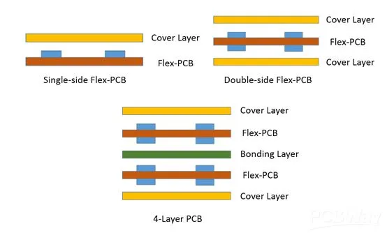
Flexible PCB Stackup: Structuring for Performance
The stackup of a flexible PCB refers to the arrangement of conductive and insulating layers. A well-designed flexible PCB stackup ensures signal integrity, mechanical stability, and manufacturability. Here’s how to approach stackup design:
- Single-Layer Stackup: Ideal for simple, low-cost designs with minimal routing needs. It consists of a single copper layer on a flexible substrate, often with a coverlay for protection. This stackup is common in static flex applications like connectors.
- Double-Layer Stackup: Provides more routing options with two copper layers separated by a dielectric. It’s suitable for moderate complexity designs, such as those in medical devices, and can handle a bending radius of about 10 times the total thickness.
- Multi-Layer Stackup: Used for high-density designs requiring complex routing, such as in aerospace systems. A 4-layer stackup might include alternating copper and dielectric layers, with stiffeners added in non-flex areas for component support. However, bending radius increases to 20-40 times the thickness due to added layers.
- Balanced Design: Ensure symmetry in the stackup to avoid uneven stress during bending. For example, in a double-layer design, place copper layers of equal thickness (e.g., 18 micrometers each) on both sides of the dielectric to maintain balance.
- Stiffeners: Add rigid materials like FR4 or polyimide stiffeners in areas where components are mounted. A typical stiffener thickness of 0.2 to 0.5 mm provides support without significantly increasing weight.
A properly configured stackup minimizes signal interference and mechanical failure. For high-speed applications, consider controlled impedance by maintaining consistent dielectric thickness (e.g., 50 micrometers for a 50-ohm impedance line) between copper layers.
Applications of Flexible PCBs Across Industries
Flexible PCBs are transforming industries by enabling innovative designs that rigid boards can’t match. Here are some key applications where they shine:
- Wearable Technology: Devices like smartwatches and fitness trackers rely on flexible PCBs to conform to curved shapes. Their lightweight nature (often under 1 gram for small designs) and dynamic bending capability make them perfect for wrist-worn gadgets.
- Medical Devices: Flexible PCBs are used in implantable devices and diagnostic tools due to their biocompatibility and ability to fit into compact spaces. For instance, a flexible circuit in a hearing aid can be folded to fit inside a 10 mm casing.
- Automotive Systems: Sensors and control units in vehicles use flexible PCBs to withstand vibration and fit into tight dashboard spaces. They often operate in temperatures ranging from -40°C to 85°C, requiring robust materials like polyimide.
- Aerospace: Satellites and drones benefit from the weight savings of flexible PCBs, which can reduce payload by up to 50% compared to rigid boards in some applications. Multi-layer stackups handle complex signal routing in these systems.
- Consumer Electronics: Smartphones and foldable devices use flexible PCBs to connect displays and components across hinges, supporting bending radii as tight as 2 mm in premium designs.
These examples highlight the versatility of flexible PCBs, making them a go-to choice for engineers tackling space constraints and dynamic requirements.

Benefits and Challenges of Flexible PCBs
Flexible PCBs offer numerous advantages, but they also come with unique challenges. Understanding both sides helps engineers make informed decisions.
Benefits
- Space and Weight Savings: They can reduce device size by up to 60% and weight by 75% compared to rigid boards, ideal for portable electronics.
- Improved Reliability: With fewer connectors and solder joints, flexible PCBs lower the risk of failure, achieving failure rates as low as 0.1% in some applications.
- Cost Efficiency: By reducing assembly steps, they can cut manufacturing costs by 20-30% in high-volume production.
Challenges
- Higher Initial Cost: Design and material costs for flexible PCBs can be 2-3 times higher than rigid boards, especially for low-volume runs.
- Complex Design Process: Accounting for bending and stress requires advanced simulation tools and prototyping, adding 10-20% more time to the design phase.
- Limited Repairability: Damaged flexible PCBs are harder to repair due to their thin, delicate structure.
Balancing these factors is key to deciding if flexible PCBs are the right fit for your project.
Tips for Successful Flexible PCB Implementation
To wrap up, here are actionable tips to ensure your flexible PCB project succeeds:
- Start with thorough prototyping to test bending radius and material durability under real-world conditions.
- Collaborate closely with your manufacturing partner to align design rules with their capabilities, ensuring trace widths and stackup configurations are feasible.
- Use simulation software to analyze stress points and signal integrity, especially for high-speed or multi-layer designs.
- Prioritize material selection based on your application’s thermal, mechanical, and electrical needs.
- Plan for stiffeners early in the design to support components and prevent solder joint failure.
By following these steps, you’ll be well-equipped to leverage the full potential of flexible PCBs in your next project.
Conclusion: Embrace the Future with Flexible PCBs
Flexible PCBs are a game-changer for modern electronics, offering unmatched design freedom and adaptability. By mastering flexible PCB design rules, understanding bending radius limits, selecting the right materials, and optimizing stackup configurations, you can create innovative, reliable products that stand out in the market. Whether you’re working on wearables, medical devices, or aerospace systems, the principles covered in this guide will help you navigate the complexities of flexible PCB design with confidence.
Ready to unlock new possibilities in your designs? Start exploring flexible PCB solutions today and push the limits of what’s possible in electronic engineering.


