ALLPCB


When designing a printed circuit board (PCB), one of the most critical factors for ensuring functionality and reliability is maintaining the right clearance between traces. PCB trace clearance, often referred to as minimum trace spacing, is the distance between conductive paths on a board. Proper spacing prevents electrical shorts, reduces interference, and ensures signal integrity, especially in high-speed or high-voltage designs. In this comprehensive guide, we’ll explore why minimum trace spacing matters, the design rules to follow, and how it impacts signal integrity and crosstalk prevention for optimal PCB performance.
What Is PCB Trace Clearance and Why Does It Matter?
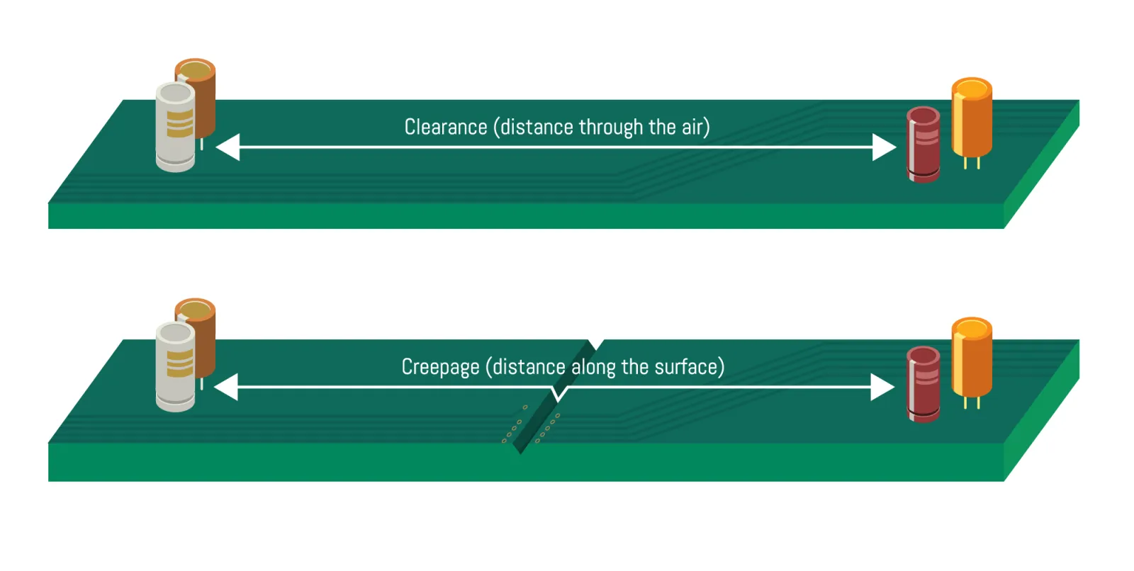
PCB trace clearance is the physical distance between two conductive elements, such as traces, pads, or vias, on a circuit board. This spacing is crucial because it directly affects the board's safety, performance, and manufacturability. If traces are too close, you risk electrical arcing, short circuits, or interference between signals, which can lead to system failures. On the other hand, overly wide spacing can waste valuable board space, making the design less efficient.
For engineers and designers, understanding and implementing minimum trace spacing is a balancing act. It ensures that the PCB operates reliably under various conditions, whether it’s a simple low-power circuit or a complex high-speed design. Factors like voltage levels, signal speed, and environmental conditions all play a role in determining the ideal clearance. By adhering to proper PCB design rules, you can prevent issues like crosstalk and maintain signal integrity, which we’ll dive into later in this post.
The Basics of Minimum Trace Spacing in PCB Design
Minimum trace spacing refers to the smallest allowable distance between two conductive elements as defined by PCB design rules. This spacing varies depending on the type of design and its requirements. For instance, a low-voltage consumer device might need only a few mils (thousandths of an inch) of clearance, while a high-voltage industrial application could require several millimeters to prevent arcing.
The primary reasons for maintaining proper trace spacing include:
- Safety: Prevents electrical shorts or arcing, especially in high-voltage designs where larger clearances (often 0.1mm per 100V as a rough guideline) are needed.
- Signal Integrity: Reduces interference between adjacent traces, ensuring signals remain clear and undistorted, particularly in high-speed circuits operating at frequencies above 100 MHz.
- Manufacturability: Ensures the PCB can be fabricated without defects, as overly tight spacing can lead to production errors during etching or soldering.
Design rules for trace spacing are often guided by industry standards like those from the Institute of Printed Circuits (IPC). For example, IPC-2221, a widely used standard, provides guidelines for clearances based on voltage levels. For a 50V circuit, a minimum clearance of 0.6mm (approximately 24 mils) might be recommended on an external layer, while higher voltages demand more space.
Factors Influencing PCB Trace Clearance
Several factors determine the minimum clearance required between traces. Understanding these can help you make informed decisions during the design phase for optimal PCB performance.
1. Voltage Levels
The voltage difference between adjacent traces is a primary factor. Higher voltages increase the risk of electrical breakdown or arcing through the air or across the board’s surface. As a general rule, clearance should increase with voltage. For instance, a design with 100V might require at least 1mm of spacing, while a 500V application could need 2.5mm or more, depending on the board material and environment.
2. Signal Speed and Frequency
In high-speed designs, signal integrity becomes a critical concern. High-frequency signals, such as those above 1 GHz, can couple with nearby traces if spacing is too tight, leading to crosstalk. To prevent this, designers often use wider spacing or add ground planes between high-speed traces. A common rule of thumb is to maintain a spacing of at least three times the trace width for high-speed signals to minimize interference.
3. Environmental Conditions
Environmental factors like humidity, temperature, and altitude can affect the required clearance. In high-humidity areas, moisture can reduce the insulating properties of the air or board material, increasing the risk of arcing. For such conditions, designers might increase clearance by 20-30% beyond standard recommendations to ensure reliability.
4. Board Material and Layer Stackup
The type of substrate material, such as FR-4, and the PCB’s layer configuration also influence clearance requirements. Internal layers often have tighter spacing due to the insulating material between them, while external layers require more clearance due to exposure to air and potential contaminants. For example, internal layer clearance for a 50V circuit might be as low as 0.1mm, compared to 0.6mm on external layers.
PCB Design Rules for Minimum Trace Spacing
To achieve optimal PCB performance, following established design rules for trace spacing is essential. These rules act as a blueprint for creating reliable and efficient designs. Below are some key guidelines to consider:
- Adhere to Industry Standards: Use standards like IPC-2221 for general clearance guidelines. For a 150V design, this standard suggests a minimum clearance of 0.7mm on external layers under typical conditions.
- Account for Manufacturing Limits: Check with your PCB fabrication house for their minimum spacing capabilities. Many standard processes can handle 6-mil (0.15mm) spacing, but tighter designs may require advanced manufacturing techniques.
- Differentiate Between Net Classes: Assign different clearance rules to different types of signals. For example, power traces might need 0.5mm spacing, while high-speed data lines could require 1mm or more to prevent crosstalk.
- Use Design Software Tools: Modern PCB design software often includes built-in design rule checks (DRC) to flag clearance violations. Set up rules based on your project’s voltage, frequency, and environmental needs.
By following these PCB design rules, you can avoid common pitfalls and ensure your board meets both functional and safety requirements.
Signal Integrity and Crosstalk Prevention Through Proper Spacing
Signal integrity refers to the quality and reliability of electrical signals as they travel through a PCB. Poor signal integrity can result in data errors, timing issues, or complete system failure, especially in high-speed applications. One of the main causes of signal degradation is crosstalk, which occurs when signals from one trace interfere with another due to inadequate spacing.
To maintain signal integrity and prevent crosstalk, consider the following strategies related to trace clearance:
1. Increase Spacing for High-Speed Signals
For high-speed signals, such as those in USB 3.0 or DDR memory circuits, maintaining a spacing of at least three times the trace width (often called the 3W rule) helps reduce electromagnetic coupling. For a 5-mil wide trace, this means a minimum spacing of 15 mils. This spacing minimizes the electric and magnetic fields that cause crosstalk.
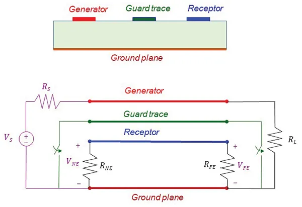
2. Use Ground Planes or Guard Traces
Placing a ground plane or a grounded guard trace between high-speed signals can further reduce interference. A guard trace, typically spaced at least 5 mils from the signal traces, acts as a shield, absorbing unwanted electromagnetic energy. This is particularly useful in designs with frequencies exceeding 500 MHz.
3. Route Critical Signals on Separate Layers
If board space is limited, consider routing high-speed or sensitive signals on different layers with a ground plane in between. This increases effective clearance and isolates signals, preserving integrity. For instance, separating a 2.4 GHz RF signal from a digital control line can prevent interference that would occur with only 0.2mm of spacing on the same layer.
Common Mistakes in PCB Trace Clearance and How to Avoid Them
Even experienced designers can make errors when setting trace clearances. Here are some common mistakes and tips to avoid them:
- Ignoring Voltage Ratings: Failing to account for peak voltages can lead to insufficient clearance and arcing. Always design for the maximum expected voltage, adding a safety margin of 10-20% to the recommended spacing.
- Overlooking High-Speed Needs: Not increasing spacing for high-frequency signals often results in crosstalk. Use simulation tools to predict interference and adjust spacing accordingly.
- Neglecting Fabrication Limits: Designing with clearances below the manufacturer’s capabilities can cause production failures. For standard boards, avoid spacing below 6 mils (0.15mm) unless you’ve confirmed advanced capabilities.
Practical Tips for Optimizing PCB Trace Clearance
Designing with optimal trace clearance doesn’t have to be overwhelming. Here are some actionable tips to streamline the process:
- Start with a Clearance Matrix: Create a table of clearance requirements based on voltage, signal type, and layer. For example, set 0.3mm for low-voltage signals on internal layers and 1mm for high-voltage traces on external layers.
- Leverage Simulation Tools: Use software to simulate electric fields and signal behavior. This can help identify potential crosstalk issues before fabrication.
- Iterate and Test: Build prototypes to test your design under real-world conditions. Measure signal integrity with an oscilloscope to confirm that clearance choices are effective.
Conclusion: Mastering PCB Trace Clearance for Better Designs
Understanding and implementing minimum clearance between traces is a cornerstone of effective PCB design. By prioritizing proper trace spacing, you can enhance signal integrity, prevent crosstalk, and ensure the safety and reliability of your circuits. Whether you’re working on a low-power gadget or a high-speed communication device, following PCB design rules and considering factors like voltage, signal frequency, and environmental conditions will lead to optimal performance.
With the right approach to PCB trace clearance, you can avoid common design errors and create boards that meet both functional and manufacturing requirements. Keep these guidelines in mind during your next project to achieve a balance between efficiency and reliability, ensuring your designs stand the test of time.