 ALLPCB


If you're dealing with silkscreen alignment issues in PCB manufacturing, you're not alone. These problems, such as misalignment, offset, or blurring, can lead to costly delays and rework. The good news? Most silkscreen defects can be fixed or prevented with the right approach. Common causes include improper setup of printing equipment, design file errors, or material inconsistencies. This guide will walk you through identifying silkscreen misalignment causes, correcting silkscreen offset, fixing silkscreen blurring, and ensuring silkscreen quality control to avoid future printing defects and minimize PCB rework.
In this comprehensive blog post, we'll dive deep into the world of silkscreen printing on printed circuit boards (PCBs). Whether you're an engineer, designer, or manufacturer, you'll find practical tips and step-by-step solutions to tackle these challenges head-on. Let’s get started.
What Is Silkscreen in PCB Manufacturing?
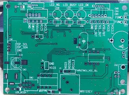
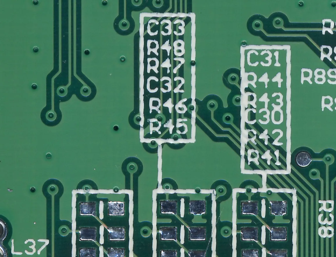
Silkscreen, often called legend printing, is a non-conductive ink layer applied to the surface of a PCB. It includes text, symbols, and markings that help identify components, test points, pin numbers, and other critical information. This layer is essential for assembly, troubleshooting, and maintenance, as it acts as a visual guide for technicians and engineers.
Typically applied as one of the final steps in PCB fabrication, silkscreen must be precise. Misalignment or defects can lead to confusion during assembly, resulting in errors or even non-functional boards. With tolerances often as tight as 0.1mm in high-density designs, even a small offset can cause significant issues. Understanding how silkscreen works and why alignment matters is the first step to addressing problems effectively.
Common Silkscreen Alignment Issues in PCB Manufacturing
Silkscreen alignment issues can manifest in several ways, each with its own set of challenges. Here are the most common problems you might encounter:
- Misalignment: The silkscreen layer is offset from its intended position, making labels and symbols appear out of place relative to components or pads.
- Blurring: Text or symbols appear fuzzy or smudged, reducing readability and potentially causing errors during assembly.
- Incomplete Printing: Parts of the silkscreen are missing or faded, often due to uneven ink application or equipment issues.
- Overlapping: Markings overlap with other elements like solder mask openings or pads, obscuring critical information.
These silkscreen printing defects can lead to assembly errors, increased PCB rework time, and even scrapped boards. Identifying the root cause is crucial for implementing effective solutions.
Silkscreen Misalignment Causes: Why Does It Happen?
Understanding the reasons behind silkscreen misalignment is the key to preventing it. Here are the primary causes:
1. Design File Errors
Incorrect data in the design files, such as mismatched layers or inaccurate scaling, can lead to misalignment. For instance, if the silkscreen layer isn’t properly aligned with the board outline in the CAD software, the printed result will be offset by as much as 0.2mm or more, depending on the error.
2. Equipment Calibration Issues
Printing equipment that isn’t properly calibrated can cause offsets. If the alignment fixtures or stencils are off by even 0.05mm, the silkscreen layer may not match the board's physical features, leading to consistent misalignment across an entire batch.
3. Material Shrinkage or Expansion
PCBs are made from materials like FR-4, which can shrink or expand slightly (up to 0.1% in some cases) due to temperature and humidity changes during manufacturing. If not accounted for, this can misalign the silkscreen relative to other layers.
4. Operator Error
Human error during setup, such as incorrect loading of boards or stencils, can introduce deviations. A misalignment of just 0.1mm might seem minor, but it can render text unreadable on densely packed boards.
5. Poor Stencil or Screen Quality
Worn-out or low-quality stencils can distort the silkscreen pattern, leading to blurring or incomplete prints. This is especially common in high-volume production where stencils endure heavy wear.
Correcting Silkscreen Offset: Step-by-Step Solutions
Once you've identified a silkscreen offset, the next step is to correct it. Here's how to address this issue effectively:
Step 1: Verify Design Files
Start by double-checking your design files. Ensure that the silkscreen layer aligns perfectly with the board outline and other layers like the solder mask. Use design rule checks (DRC) in your CAD software to catch errors before sending files for production. Correcting a digital offset of 0.15mm in the design phase can save hours of rework later.
Step 2: Calibrate Equipment
Work with your manufacturing team to ensure that printing machines are calibrated. Check alignment fixtures and stencils for wear or damage. A calibration adjustment of as little as 0.05mm can make a significant difference in print accuracy.
Step 3: Adjust for Material Properties
Account for potential material shrinkage or expansion by adding a small tolerance (e.g., 0.1%) to your design. Consult with your manufacturer about environmental conditions during production to minimize these effects.
Step 4: Test with a Prototype
Before full-scale production, create a prototype to test silkscreen alignment. Measure the offset using precision tools like a digital caliper or microscope. If an offset of 0.2mm is detected, adjust the setup accordingly before proceeding with the batch.
Fixing Silkscreen Blurring: Tips for Clear Markings
Blurring is another common issue that affects silkscreen readability. Here’s how to tackle it:
1. Optimize Ink Viscosity
Blurring often occurs when the ink is too thin or too thick. Work with your manufacturer to ensure the ink viscosity is within the recommended range (typically 500-1000 centipoise for most silkscreen inks) to achieve crisp prints.
2. Check Printing Speed and Pressure
Excessive printing speed or uneven pressure can cause smudging. Adjust the machine settings to a moderate speed (e.g., 50-100mm per second) and ensure uniform pressure across the stencil to prevent ink spread.
3. Use High-Quality Stencils
Invest in durable, high-resolution stencils to avoid distortion. A stencil with a mesh count of 200-300 per inch can provide finer detail and reduce blurring compared to lower-quality options.
4. Inspect Surface Cleanliness
Ensure the PCB surface is free of dust, oil, or residue before printing. Even a thin layer of contamination can cause ink to spread, resulting in blurred text or symbols.
Silkscreen Quality Control: Preventing Defects Before They Happen
Prevention is always better than correction. Implementing robust silkscreen quality control measures can save time and resources in the long run. Here are some best practices:
1. Pre-Production Checks
Before starting production, verify all design files and manufacturing setups. Use automated optical inspection (AOI) systems to detect alignment issues with an accuracy of up to 0.01mm.
2. Standard Operating Procedures (SOPs)
Establish clear SOPs for operators to follow during setup and printing. This includes guidelines for stencil alignment, ink preparation, and machine calibration to minimize human error.
3. Regular Equipment Maintenance
Schedule routine maintenance for printing equipment to prevent gradual misalignment or wear. Replace stencils after a set number of cycles (e.g., every 10,000 prints) to maintain quality.
4. Batch Sampling
Inspect a small sample from each batch using magnification tools to check for defects like blurring or offset. Catching a 0.1mm misalignment early can prevent an entire batch from being scrapped.
PCB Rework for Silkscreen Defects: When and How to Fix
Sometimes, despite best efforts, silkscreen defects slip through. When this happens, PCB rework may be necessary. Here’s how to approach it:
Assess the Severity
Determine if the defect affects functionality or assembly. A minor offset of 0.1mm might not require rework if the markings are still readable. However, severe blurring or missing labels may necessitate correction.
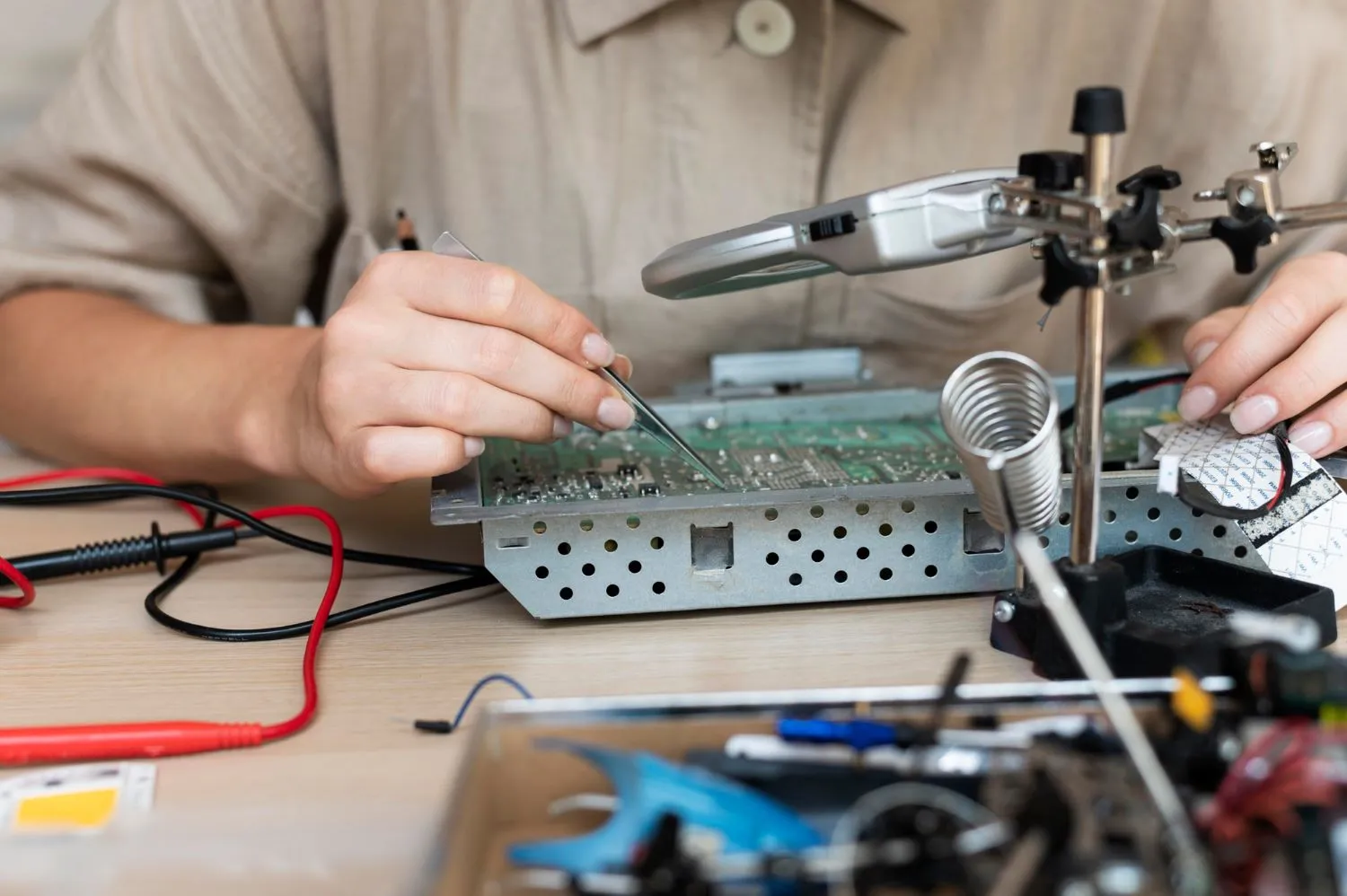
Manual Touch-Up
For small batches, manual touch-up using fine-tip pens with PCB-safe ink can correct minor issues like faded text. This method works best for low-volume or prototype boards.
Reprinting the Silkscreen Layer
For larger issues, consider stripping the existing silkscreen layer (if possible) and reprinting it. This process requires precision to avoid damaging other layers like the solder mask and should only be done by experienced technicians.
Document and Learn
After rework, document the issue and solution to prevent recurrence. For example, if a 0.2mm offset was caused by a calibration error, update the SOP to include a pre-run alignment check.
Design Tips to Avoid Silkscreen Printing Defects
A well-thought-out design can prevent many silkscreen issues from occurring. Keep these tips in mind during the design phase:
- Use Appropriate Font Sizes: Stick to a minimum font size of 6 points (about 1mm height) to ensure readability after printing.
- Avoid Critical Areas: Don’t place silkscreen markings over solder pads or vias, as this can lead to overlap or incomplete printing.
- Simplify Markings: Use simple shapes and text to reduce the risk of blurring or distortion during printing.
- Provide Clear Layer Data: Ensure your silkscreen layer is clearly defined in the design files, with no overlap between elements.
Partnering with a Reliable Manufacturer for Silkscreen Precision
Choosing a manufacturing partner with advanced equipment and strict quality control processes can make a big difference in silkscreen accuracy. Look for a provider that uses automated alignment systems with tolerances as tight as 0.05mm and offers pre-production prototypes to catch issues early. Clear communication about your design requirements and expectations is also key to avoiding defects.
Conclusion: Mastering Silkscreen Alignment for Flawless PCBs
Silkscreen alignment issues in PCB manufacturing can be frustrating, but they’re not insurmountable. By understanding silkscreen misalignment causes, correcting silkscreen offset with precise adjustments, fixing silkscreen blurring through optimized processes, and enforcing silkscreen quality control, you can minimize printing defects and reduce the need for PCB rework. Start with a solid design, implement strict quality checks, and partner with a trusted manufacturer to ensure your PCBs are both functional and visually clear.
With the practical steps and tips outlined in this guide, you’re well-equipped to tackle silkscreen challenges and achieve high-quality results in your next project. Remember, precision in every layer—down to 0.1mm—can make all the difference in delivering reliable, professional-grade PCBs.


