ALLPCB


If you're diving into the world of high-density printed circuit boards (HDI PCBs), you’ve likely come across the term "stacked vias." But what exactly are they, and why are they so crucial in modern electronics design? In this comprehensive guide, we’ll break down everything you need to know about stacked vias, from design tips to manufacturing processes, reliability concerns, and cost analysis. Whether you're an engineer or a designer, this stacked via design guide will help you master HDI PCB stacked via technology for your next project.
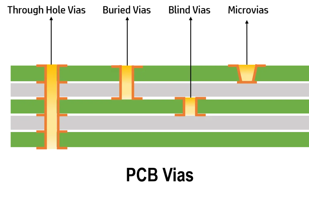
At its core, a stacked via is a vertical interconnect structure in an HDI PCB where multiple vias are stacked on top of each other to connect different layers of the board. This technique saves space, improves signal integrity, and enables the creation of smaller, more complex devices. Now, let’s explore the details of stacked vias, including their benefits, challenges, and best practices.
What Are Stacked Vias in HDI PCBs?
Stacked vias are a key feature in high-density interconnect (HDI) PCBs, which are designed to pack more functionality into smaller spaces. Unlike traditional through-hole vias that go all the way through the board, stacked vias consist of smaller microvias that connect only specific layers. These microvias are placed directly on top of each other, forming a "stack" that allows for efficient routing in multi-layer boards.
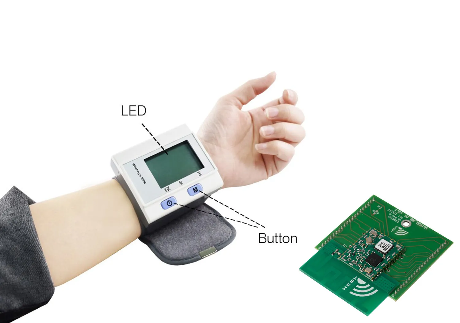
In HDI PCB stacked via structures, microvias are often filled with conductive material, typically copper, to ensure reliable electrical connections. This design is especially useful for complex devices like smartphones, tablets, and medical equipment, where space is limited, and performance is critical.
Why Use Stacked Vias in High-Density PCBs?
Stacked vias offer several advantages that make them a go-to choice for modern PCB designs. Here are some of the main reasons engineers opt for this technology:
- Space Savings: By stacking vias, you can reduce the board’s footprint, allowing for more compact designs. This is critical in applications like wearable devices, where every millimeter counts.
- Improved Signal Integrity: Stacked vias minimize the length of signal paths, reducing impedance and signal loss. For high-speed signals operating at frequencies above 1 GHz, this can significantly enhance performance.
- Higher Layer Density: Stacked vias enable connections between multiple layers without the need for larger through-hole vias, supporting designs with 8, 10, or even more layers in a single board.
- Enhanced Design Flexibility: With stacked vias, designers can route traces more efficiently, avoiding congestion in densely packed layouts.
However, while stacked vias bring many benefits, they also come with challenges, such as increased manufacturing complexity and costs, which we’ll discuss later in this guide.
Stacked Via Design Guide: Best Practices for HDI PCBs
Designing with stacked vias requires careful planning to ensure functionality and manufacturability. Below are some key guidelines to follow when incorporating HDI PCB stacked via structures into your design:
1. Understand Your Layer Stack-Up
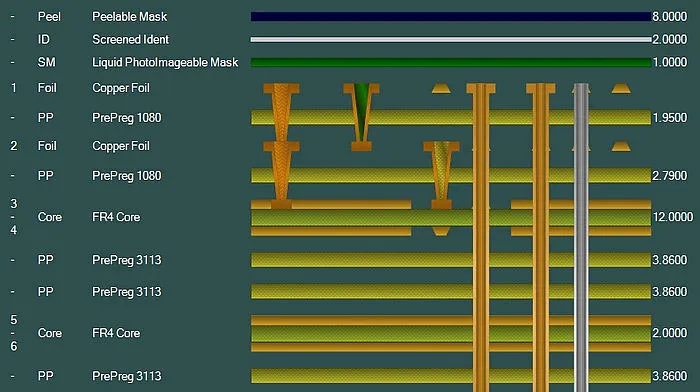
Before placing stacked vias, map out your PCB’s layer stack-up. Determine how many layers need to be connected and where the vias will be placed. For example, a common HDI stack-up might include 2+N+2 layers, where "N" represents the core layers, and the additional layers are built up with microvias. Ensure that stacked vias are only used where necessary to avoid overcomplicating the design.
2. Optimize Via Size and Aspect Ratio
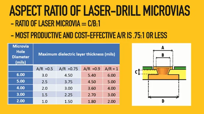
Microvias used in stacked structures typically have diameters ranging from 0.1 mm to 0.15 mm. Maintain an aspect ratio (depth-to-diameter) of 1:1 or less to ensure reliable plating during manufacturing. For instance, a microvia with a 0.1 mm diameter should not exceed 0.1 mm in depth to avoid issues like incomplete copper filling.
3. Align Stacked Vias Properly
Misalignment between stacked vias can lead to connection failures. Use precise design tools to ensure that each via in the stack is perfectly aligned with the one below it. Modern design software often includes features to check via alignment and prevent errors during layout.
4. Consider Signal Integrity
For high-speed designs, stacked vias can introduce parasitic capacitance and inductance, affecting signal integrity. Keep the stack height to a minimum (e.g., no more than 2-3 vias in a stack) to reduce these effects. Additionally, place ground planes near high-speed signals to minimize interference.
Stacked Via Manufacturing Process: How Are They Made?
The manufacturing process for stacked vias in HDI PCBs is more complex than for traditional through-hole vias. It involves multiple steps to ensure precision and reliability. Here’s a simplified overview of the stacked via manufacturing process:
1. Layer Build-Up
HDI PCBs are built using a sequential lamination process. Thin layers of dielectric material and copper are added one at a time to create the multi-layer structure. Each layer is carefully aligned to ensure proper placement of vias.
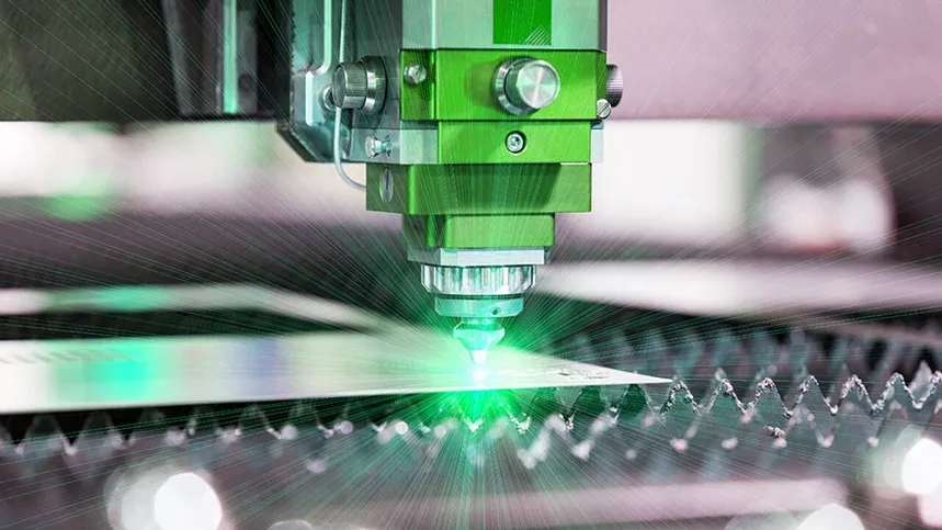
2. Microvia Drilling
Microvias are created using laser drilling, which allows for precise holes with diameters as small as 0.1 mm. Laser drilling is preferred over mechanical drilling because it produces cleaner, more accurate holes without damaging surrounding materials.
3. Copper Plating and Filling
After drilling, the microvias are plated with copper to establish electrical connections. In stacked via designs, the vias are often filled with copper to provide a solid connection and prevent voids that could weaken the structure. This step is critical for ensuring long-term reliability.
4. Stacking and Lamination
Once the microvias are formed and filled, additional layers are laminated on top, and the process repeats for each via stack. Precision is key to avoid misalignment, which could lead to open circuits or poor connections.
Stacked Via Reliability: Challenges and Solutions
While stacked vias offer many benefits, their reliability can be a concern if not designed or manufactured properly. Here are some common challenges related to stacked via reliability, along with solutions to address them:
1. Thermal Stress
During operation, PCBs are exposed to temperature changes that can cause thermal expansion. Stacked vias, due to their small size and multi-layer structure, are more prone to cracking under thermal stress. To mitigate this, use materials with similar coefficients of thermal expansion (CTE) for the dielectric and copper layers. For example, selecting a dielectric material with a CTE close to 17 ppm/°C (the CTE of copper) can reduce stress.
2. Copper Filling Defects
Incomplete copper filling or voids in stacked vias can lead to weak connections and eventual failure. Manufacturers often use advanced plating techniques and X-ray inspection to detect and prevent voids. As a designer, ensure that via aspect ratios are within recommended limits to facilitate proper filling.
3. Misalignment Issues
Misaligned vias in a stack can result in poor electrical connections. This is often a manufacturing issue, but designers can help by providing clear design files and specifying tight tolerances for via placement (e.g., ±0.05 mm).
By addressing these challenges, you can significantly improve the reliability of stacked vias in your HDI PCB designs. Always collaborate closely with your manufacturing partner to ensure that design specifications are feasible and aligned with their capabilities.
Stacked Via Cost Analysis: Are They Worth the Investment?
One of the biggest considerations when using stacked vias in HDI PCBs is cost. While they enable smaller, more powerful designs, they also increase manufacturing expenses. Let’s break down the factors that contribute to the cost of stacked vias and help you decide if they’re worth the investment.
Factors Affecting Stacked Via Costs
- Number of Layers: More layers mean more sequential build-up steps, increasing both material and labor costs. For example, a 10-layer HDI board with stacked vias can cost 30-50% more than a 6-layer board with simpler via structures.
- Microvia Complexity: Stacked vias require precise laser drilling and copper filling, which are more expensive than traditional mechanical drilling. The smaller the via (e.g., 0.1 mm vs. 0.2 mm), the higher the cost due to tighter tolerances.
- Material Selection: High-performance materials that withstand thermal stress and support fine features often come at a premium. For instance, using advanced dielectric materials can add 10-20% to the overall cost.
- Volume and Yield: Low-volume production runs are more expensive per unit because setup costs are spread over fewer boards. Additionally, complex designs with stacked vias may have lower yields due to manufacturing defects, further driving up costs.
Balancing Cost and Performance
While stacked vias can be costly, they often provide value by enabling smaller, more efficient designs. For high-end applications like aerospace or medical devices, the performance benefits usually outweigh the added expense. However, for cost-sensitive projects, consider alternatives like staggered vias (where vias are offset rather than stacked) to reduce complexity and save on manufacturing costs.
Applications of Stacked Vias in Modern Electronics
Stacked vias are widely used in industries where compact, high-performance electronics are essential. Some common applications include:
- Consumer Electronics: Smartphones, tablets, and wearables rely on HDI PCBs with stacked vias to fit powerful components into tiny spaces.
- Automotive Systems: Advanced driver-assistance systems (ADAS) and infotainment units use stacked vias for reliable, high-speed signal transmission.
- Medical Devices: Portable diagnostic tools and implantable devices benefit from the compact size and reliability of stacked via designs.
- Aerospace and Defense: High-density interconnects with stacked vias support the complex, mission-critical electronics used in satellites and military equipment.
These applications highlight the versatility and importance of stacked vias in pushing the boundaries of electronic design.
Tips for Collaborating with Manufacturers on Stacked Via Designs
Successful implementation of stacked vias requires close collaboration with your PCB manufacturer. Here are some tips to ensure a smooth process:
- Share Detailed Design Files: Provide clear, accurate design files that include via specifications, layer stack-up details, and material requirements.
- Discuss Capabilities Early: Not all manufacturers have the equipment or expertise to handle complex stacked via designs. Confirm their capabilities, such as minimum via size and stacking limits, before finalizing your design.
- Request Design for Manufacturability (DFM) Feedback: Many manufacturers offer DFM reviews to identify potential issues in your design, such as via alignment or aspect ratio concerns, before production begins.
- Plan for Testing: Work with your manufacturer to establish testing protocols, such as X-ray inspection for void detection, to ensure the reliability of stacked vias.
Conclusion: Mastering Stacked Vias for HDI PCB Success
Stacked vias are a game-changer in the world of high-density PCBs, enabling smaller, faster, and more powerful electronic devices. By following the best practices outlined in this stacked via design guide, you can optimize your HDI PCB stacked via layouts for performance and manufacturability. While challenges like reliability and cost must be carefully managed, the benefits of stacked vias often make them a worthwhile choice for cutting-edge applications.
From understanding the stacked via manufacturing process to addressing reliability concerns and conducting a thorough cost analysis, this guide has covered the essentials to help you succeed. Armed with this knowledge, you’re ready to tackle the complexities of HDI PCB design and bring your innovative ideas to life.