 ALLPCB


Choosing the right layer thickness for your printed circuit board (PCB) is a critical decision that impacts performance, durability, and manufacturability. Whether you're designing a simple prototype or a complex multilayer board, understanding factors like standard PCB thickness, PCB thickness tolerance, and PCB material thickness can make or break your project. In this comprehensive guide, we'll walk you through everything you need to know to select the optimal layer thickness for your PCB, including tips on using a PCB thickness calculator and designing an effective PCB layer stackup.
At the heart of PCB design, layer thickness affects electrical performance, mechanical strength, and PCB thermal management. A common starting point is the standard PCB thickness of 1.6 mm (0.063 inches), but this isn't a one-size-fits-all solution. Depending on your application, you might need thinner or thicker boards, and understanding the nuances of PCB thickness tolerance and material properties is essential. Let's dive into the details to help you make an informed choice for your next project.
Why PCB Layer Thickness Matters
The thickness of your PCB and its individual layers plays a significant role in how well your board performs. A board that's too thin might lack the mechanical strength to withstand physical stress, while one that's too thick could increase costs unnecessarily or affect signal integrity. Here are the key reasons why selecting the right layer thickness is crucial:
- Electrical Performance: Layer thickness impacts impedance control, especially in high-frequency designs. Thinner dielectric layers can reduce impedance, while thicker ones might be needed for high-voltage applications to prevent breakdown.
- Mechanical Stability: Thicker boards offer better durability, which is vital for applications exposed to vibration or mechanical stress, such as automotive or industrial electronics.
- Thermal Management: The thickness of copper layers and the overall board affects heat dissipation. Thicker copper can handle higher currents without overheating, improving reliability.
- Cost and Manufacturability: Non-standard thicknesses can increase manufacturing costs and lead times. Sticking to standard PCB thickness values often ensures smoother production.
Understanding Standard PCB Thickness
One of the first things to consider when designing a PCB is the standard thickness. The most widely used standard PCB thickness is 1.6 mm (0.063 inches), a value that has become an industry norm due to its balance of strength, cost, and compatibility with most components and mounting hardware. However, this isn't a rigid rule, and other common thicknesses include 0.8 mm, 1.0 mm, 2.0 mm, and even up to 3.2 mm for specialized applications.
Standard thicknesses are often preferred because they align with widely available materials and manufacturing processes. Choosing a non-standard thickness, such as 1.2 mm, might be possible but could result in higher costs or delays due to the need for custom materials or adjusted production setups.
For most designs, starting with a standard PCB thickness like 1.6 mm is a safe bet. However, if your project has specific requirements—such as fitting into a tight enclosure or handling high currents—you'll need to evaluate whether a different thickness is necessary.
Factors Influencing PCB Layer Thickness Selection
Selecting the right layer thickness isn't just about picking a number. Several factors come into play, and understanding these will help you make an informed decision. Let's break them down:
1. Application and Environment
The intended use of your PCB heavily influences the required thickness. For instance, consumer electronics like smartphones often use thinner boards (0.8 mm or less) to save space, while industrial or automotive applications might require thicker boards (2.0 mm or more) for added durability against harsh conditions like vibration or temperature extremes.
2. Number of Layers and Stackup Design
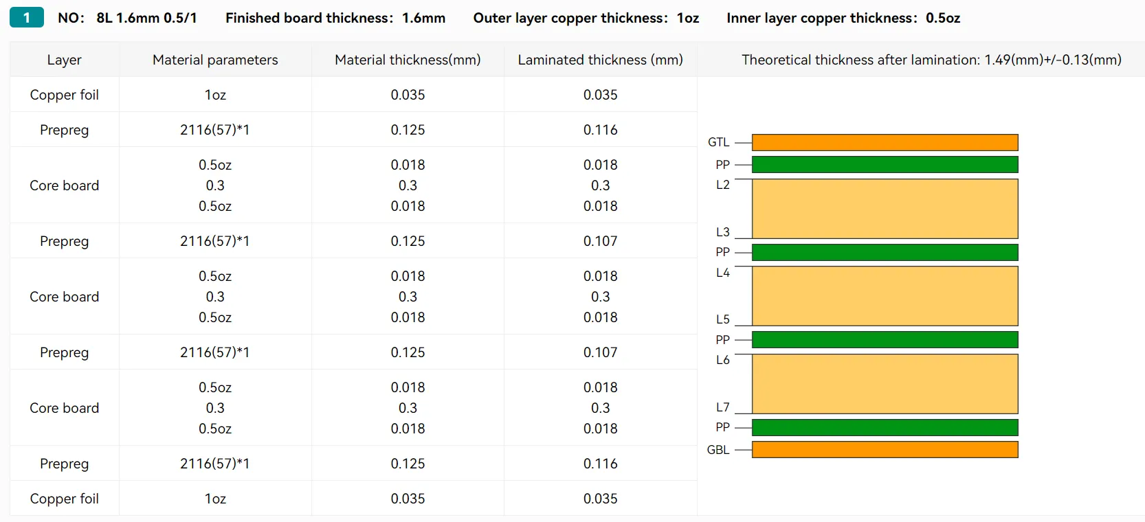
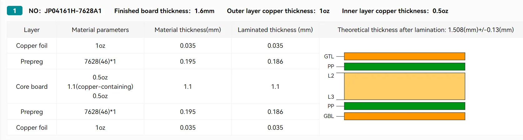
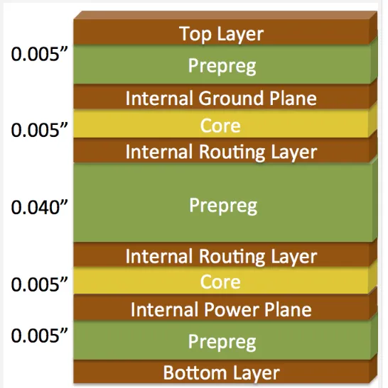
The PCB layer stackup—the arrangement of copper and dielectric layers—directly affects the overall thickness. A 2-layer board might be as thin as 0.8 mm, while a 6-layer or 8-layer board could easily reach 1.6 mm or more due to the additional layers. When designing your PCB layer stackup, consider the dielectric thickness between layers, as this impacts signal integrity and impedance. For high-speed designs, thinner dielectric layers (e.g., 0.1 mm) might be needed to maintain controlled impedance values like 50 ohms, a common standard for RF signals.
3. Current Carrying Capacity
The thickness of copper layers, often measured in ounces per square foot (oz/ft2), determines how much current a trace can handle. A standard 1 oz copper layer is about 0.035 mm thick and can carry approximately 1-2 amps per 10-mil-wide trace at room temperature. For higher currents, you might need 2 oz (0.07 mm) or even 3 oz copper, which increases the overall board thickness. Balancing PCB copper thickness with thermal performance is key to preventing overheating.
4. Signal Integrity and Impedance
In high-frequency or high-speed digital designs, layer thickness affects signal integrity. The dielectric thickness between a signal layer and its reference plane (ground or power) influences the characteristic impedance of traces. For example, a 50-ohm impedance for a microstrip trace on a 1.6 mm board with a standard FR-4 material (dielectric constant of 4.5) might require a trace width of about 0.3 mm and a dielectric thickness of 0.2 mm. Adjusting layer thickness is often necessary to meet these precise requirements.
5. PCB Thickness Tolerance
Manufacturing processes aren't perfect, and PCB thickness tolerance refers to the acceptable variation in the final board thickness. For a standard 1.6 mm board, the tolerance might be ±10%, meaning the actual thickness could range from 1.44 mm to 1.76 mm. Tighter tolerances are possible but often come at a higher cost. When selecting your layer thickness, consider whether your design can accommodate this variation or if you need to specify a stricter tolerance for critical applications.
How to Use a PCB Thickness Calculator
Designing a PCB with the right layer thickness doesn't have to be guesswork. A PCB thickness calculator is a valuable tool that helps you determine the optimal thickness based on your design parameters. These calculators often take into account factors like the number of layers, material properties, copper weight, and dielectric thickness to provide an accurate estimate of the final board thickness.
Here's how to use a PCB thickness calculator effectively:
- Input the Number of Layers: Specify whether your board is 2-layer, 4-layer, or more. Each additional layer adds to the overall thickness.
- Select Material Properties: Choose the core and prepreg materials, such as FR-4, which have predefined dielectric thicknesses (e.g., 0.2 mm for a typical prepreg layer).
- Define Copper Thickness: Enter the copper weight (e.g., 1 oz or 2 oz) for each layer, as this impacts the total thickness.
- Review the Results: The calculator will output the estimated total thickness, helping you decide if adjustments are needed to meet your design goals.
Using a calculator simplifies the process of designing a PCB layer stackup, especially for complex multilayer boards. It ensures that your board meets both electrical and mechanical requirements without unnecessary trial and error.
Common PCB Material Thickness and Properties
The materials used in your PCB also influence layer thickness. The most common substrate material is FR-4, a fiberglass-epoxy laminate with a dielectric constant of around 4.5 and a thermal conductivity of 0.25 W/m·K. FR-4 cores and prepregs come in standard thicknesses, such as 0.1 mm, 0.2 mm, and 0.5 mm, which are combined to achieve the desired overall thickness.
For specialized applications, other materials might be used:
- High-Frequency Laminates: Materials like Rogers or Teflon have lower dielectric constants (e.g., 2.2-3.0) and are often thinner to support RF designs.
- Polyimide: Used in flexible PCBs, polyimide substrates are typically 0.05 mm to 0.1 mm thick, offering flexibility but less mechanical strength.
- Metal-Core PCBs: For high-power applications, metal-core boards use thicker substrates (1.0 mm or more) to improve heat dissipation.
Understanding PCB material thickness and properties helps you choose the right combination for your design, balancing cost, performance, and manufacturability.
Tips for Designing an Effective PCB Layer Stackup
A well-designed PCB layer stackup ensures optimal performance and reliability. Here are some practical tips to consider when planning your stackup and selecting layer thicknesses:
- Plan for Symmetry: Arrange layers symmetrically to avoid warping during manufacturing. For a 4-layer board, place two signal layers on the outside and two inner layers (ground and power) in the middle.
- Minimize Crosstalk: Use adequate dielectric thickness between signal layers to reduce interference, especially in high-speed designs.
- Optimize Ground Planes: Ensure ground planes are close to signal layers to provide a low-impedance return path, which often means using thinner dielectric layers (e.g., 0.1-0.2 mm).
- Consider Manufacturing Limits: Check with your manufacturer for minimum and maximum layer thicknesses, as well as achievable tolerances, to avoid design issues.
Common Mistakes to Avoid When Selecting PCB Thickness
Even experienced designers can make mistakes when choosing PCB layer thickness. Here are some pitfalls to watch out for:
- Ignoring Application Needs: Choosing a standard 1.6 mm thickness without considering whether your application requires a thinner or thicker board can lead to performance issues.
- Overlooking Tolerance: Failing to account for PCB thickness tolerance can result in boards that don't fit enclosures or connectors properly.
- Neglecting Thermal Effects: Underestimating the heat generated by high-current traces on thin copper layers can cause reliability problems.
- Using Non-Standard Thicknesses Unnecessarily: Opting for a custom thickness without a clear reason can increase costs and delay production.
Final Thoughts on Selecting PCB Layer Thickness
Selecting the right layer thickness for your PCB is a balancing act between electrical performance, mechanical stability, and cost. By understanding standard PCB thickness options like 1.6 mm, leveraging tools like a PCB thickness calculator, and carefully designing your PCB layer stackup, you can create a board that meets your project's unique needs. Pay attention to factors like PCB thickness tolerance and PCB material thickness to ensure manufacturability and reliability.
Whether you're working on a simple 2-layer board or a complex multilayer design, taking the time to evaluate your layer thickness choices will pay off in the long run. With the insights and tips provided in this guide, you're well-equipped to make informed decisions that enhance the performance and durability of your PCB designs. Trust in thorough planning and precise calculations to achieve the best results for your next project.


