 ALLPCB


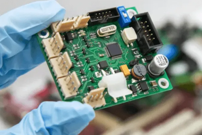
Designing printed circuit boards (PCBs) for Internet of Things (IoT) projects requires the right software to handle compact layouts, wireless connectivity, and power efficiency. If you're searching for the best PCB design software for IoT, you might be considering tools like Altium Designer, KiCad, or Eagle, or even exploring online PCB design tools. In this comprehensive guide, we’ll break down the top software options, including Altium Designer for IoT PCB, KiCad for IoT PCB, and Eagle PCB software for IoT, to help you choose the perfect tool for your project. Whether you're a hobbyist or a professional engineer, this article will provide actionable insights to streamline your design process.
Why IoT PCB Design Requires Specialized Software
IoT devices are unique because they often combine sensors, microcontrollers, and wireless modules into small, power-efficient designs. This means PCB design software for IoT must support complex multilayer boards, high-frequency signals, and integration with components like Wi-Fi or Bluetooth chips. For instance, maintaining signal integrity for a 2.4 GHz Wi-Fi module requires precise impedance control, often around 50 ohms for RF traces. Without the right tools, managing these requirements can lead to costly errors or performance issues.
Specialized software offers features like 3D visualization to check component clearance, simulation tools to test signal behavior, and libraries with IoT-specific components. In the sections below, we’ll explore how different tools cater to these needs and help you decide which one fits your project.
Key Features to Look for in IoT PCB Design Software
Before diving into specific tools, let’s cover the essential features you should prioritize when selecting software for IoT PCB design. These features ensure your designs are functional, efficient, and ready for manufacturing.
- Component Libraries: Look for extensive libraries with IoT-specific parts like ESP32 modules, sensors, and low-power ICs. A good library saves hours of manual component creation.
- Signal Integrity Tools: High-frequency signals in IoT devices (e.g., 2.4 GHz for Bluetooth) need software that can simulate and manage impedance, crosstalk, and noise.
- Multilayer Support: Many IoT designs use 4 or more layers to save space. Your software should handle complex stack-ups with ease.
- 3D Visualization: Seeing your PCB in 3D helps verify component placement and enclosure fit, especially for tiny IoT devices.
- Integration with Manufacturing: Direct export of Gerber files or integration with fabrication processes ensures a smooth transition from design to production.
- Cost and Accessibility: Depending on your budget, you might need free or affordable tools without sacrificing essential features.
With these criteria in mind, let’s explore some of the best PCB design software for IoT projects and see how they stack up.
Top PCB Design Software for IoT Projects
1. Altium Designer for IoT PCB Design
Altium Designer is often considered a premium choice for professional engineers working on IoT projects. It offers a robust set of tools tailored for complex designs, making it a go-to for Altium Designer IoT PCB workflows.
Key Strengths:
- Advanced Signal Integrity: Altium provides built-in simulation for high-speed signals, critical for IoT devices with RF components. You can analyze impedance mismatches and adjust trace widths (e.g., 0.2 mm for a 50-ohm trace) directly in the software.
- Comprehensive Libraries: It includes a vast database of components, with cloud-based libraries for the latest IoT modules like the ESP8266 or Nordic nRF series.
- 3D Integration: The 3D view lets you check if components fit within tight enclosures, a common challenge in IoT wearables or smart home devices.
- Team Collaboration: For larger projects, Altium supports multi-user design environments, ideal for teams working on IoT ecosystems.
Drawbacks: Altium Designer comes with a high price tag, often costing thousands of dollars per license. This might not be feasible for hobbyists or small startups. Additionally, its steep learning curve can be a hurdle for beginners.
Best For: Professional engineers or companies developing sophisticated IoT products with budgets to match.
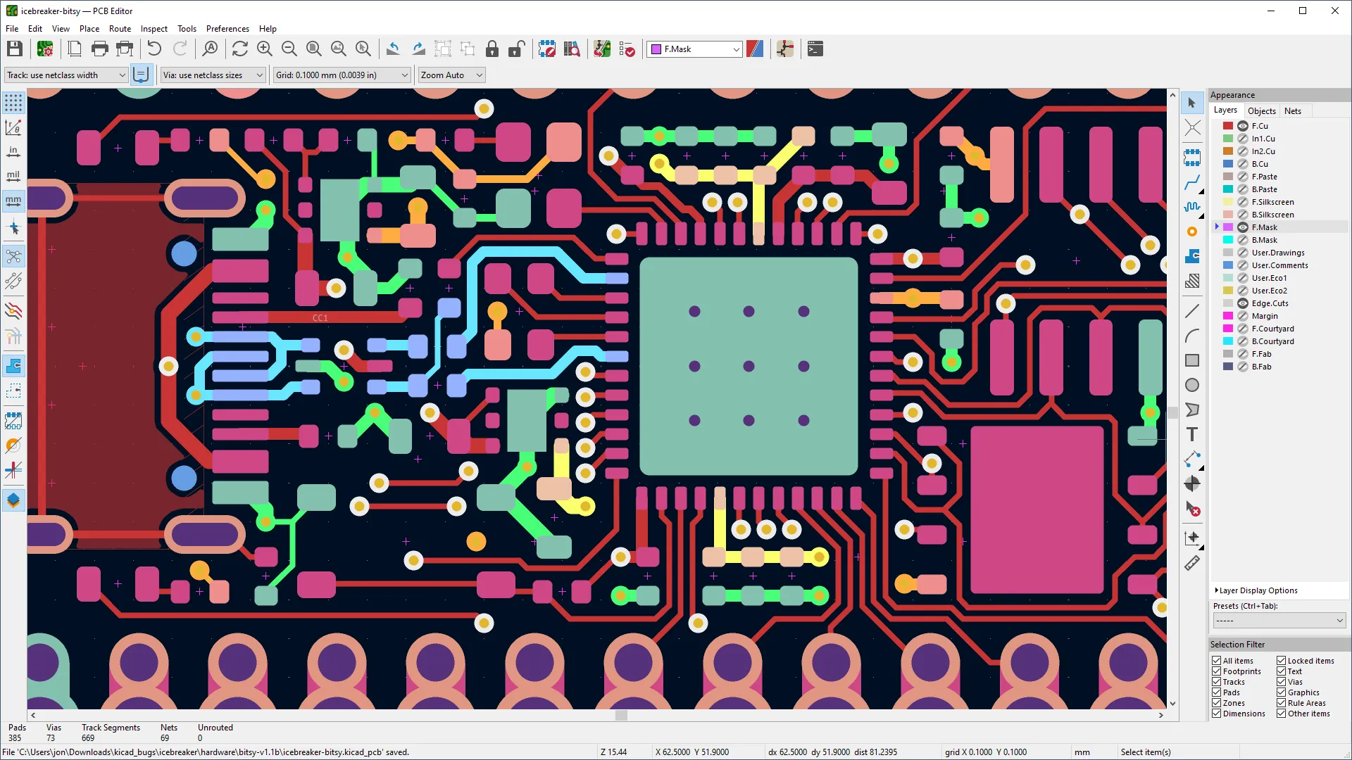
2. KiCad for IoT PCB Design
KiCad is a powerful open-source option that has gained popularity among hobbyists and professionals alike. For those searching for KiCad IoT PCB solutions, this free tool offers impressive capabilities without the cost.
Key Strengths:
- Cost-Free: KiCad is completely free, making it accessible for anyone working on IoT projects, from students to startups.
- Community Support: With a large user base, you can find tutorials and plugins for IoT-specific needs, such as custom RF layouts or panelization for mass production.
- 3D Viewer: KiCad’s 3D visualization helps ensure your compact IoT design fits within physical constraints, like a 20 mm x 20 mm board for a wearable sensor.
- Cross-Platform: Available on Windows, macOS, and Linux, KiCad works wherever you do.
Drawbacks: KiCad lacks some advanced features like native signal integrity simulation, which might require external tools for high-frequency IoT designs. Its interface can also feel less intuitive compared to paid alternatives.
Best For: Hobbyists, educators, and small teams looking for a budget-friendly yet capable tool for IoT PCB design.
3. Eagle PCB Software for IoT
Eagle has long been a favorite for electronics designers, and it remains a solid choice for Eagle PCB software IoT applications. Now part of a larger CAD ecosystem, it balances ease of use with professional features.
Key Strengths:
- User-Friendly Interface: Eagle is easier to learn than some competitors, making it a good starting point for IoT beginners.
- Component Libraries: It offers a decent library of parts, including many IoT-relevant components like microcontrollers and wireless chips.
- Integration: Eagle supports direct links to manufacturing processes, simplifying the move from design to prototype for IoT devices.
- Subscription Model: With flexible pricing, it’s more affordable than some high-end tools, though not free.
Drawbacks: Eagle’s free version has limitations on board size and layer count, which can be restrictive for complex IoT designs needing 6 or more layers. Its simulation capabilities are also less robust than other premium tools.
Best For: Intermediate designers or small businesses wanting a balance of cost and functionality for IoT projects.
4. Online PCB Design Tools for IoT
For those who prefer not to install software or need quick access across devices, online PCB design tools are a growing trend. These web-based platforms are often user-friendly and cater to IoT projects with lightweight designs.
Key Strengths:
- Accessibility: Work from any device with an internet connection, ideal for collaborative IoT projects across teams.
- No Installation: Skip the hassle of software setup and updates, saving time for fast-paced IoT prototyping.
- Cost-Effective: Many online tools offer free basic plans or low-cost subscriptions, fitting tight budgets.
- Cloud Storage: Designs are saved online, reducing the risk of data loss and enabling easy sharing.
Drawbacks: Online tools often lack advanced features like signal integrity analysis, which is critical for high-speed IoT signals. They may also have slower performance for large designs and require a stable internet connection.
Best For: Beginners or teams needing quick, simple IoT designs without complex requirements.
Comparing the Best PCB Design Software for IoT
To help you decide, here’s a quick comparison of the tools discussed based on key factors for IoT PCB design.
| Software | Cost | Signal Integrity Tools | 3D Visualization | Best For |
|---|---|---|---|---|
| Altium Designer | High (Subscription) | Excellent | Yes | Professionals |
| KiCad | Free | Limited | Yes | Hobbyists & Startups |
| Eagle | Moderate (Subscription) | Basic | Yes | Intermediate Users |
| Online Tools | Free/Low Cost | Minimal | Limited | Beginners |
This table highlights the trade-offs between cost and functionality. For instance, if your IoT project involves a high-speed 5 GHz signal, Altium’s advanced tools might be worth the investment. For a simple sensor node, KiCad or an online tool could suffice.
Tips for Optimizing IoT PCB Design with Software
Regardless of the software you choose, here are some practical tips to ensure your IoT PCB design is successful:
- Plan for Power Efficiency: Use software features to simulate power consumption. Many IoT devices run on batteries, so place decoupling capacitors (e.g., 0.1 μF) near ICs to stabilize voltage.
- Minimize RF Interference: Keep RF traces short and use ground planes to reduce noise. Software with impedance calculators can help maintain 50-ohm traces for Wi-Fi or Bluetooth signals.
- Test with Simulations: If your software supports it, run simulations to check signal behavior before prototyping. This can save costly revisions.
- Check Design Rules: Use the software’s design rule checker (DRC) to ensure spacing, trace widths (e.g., 0.15 mm for high-density areas), and via sizes meet manufacturing standards.
- Collaborate Early: If working in a team, use software with version control or cloud sharing to avoid design conflicts on IoT projects.
How to Choose the Right Software for Your IoT Project
Selecting the best PCB design software for IoT depends on your specific needs. Here’s a quick decision guide:
- Budget Constraints: If cost is a concern, start with KiCad or an online tool. They offer enough features for most small-scale IoT projects.
- Complex Designs: For multilayer boards with high-speed signals, invest in Altium Designer to access advanced simulation and routing tools.
- Learning Curve: If you’re new to PCB design, Eagle or online tools provide a gentler introduction without overwhelming features.
- Team Collaboration: For group projects, prioritize software with cloud or multi-user support, like Altium or certain online platforms.
Consider starting with a free tool to prototype your IoT idea. As your project grows in complexity, you can upgrade to a paid solution if needed.
Conclusion: Streamline Your IoT PCB Design with the Right Tool
Designing PCBs for IoT projects is a challenging but rewarding process, and the software you choose plays a huge role in your success. Whether you opt for the powerful features of Altium Designer for IoT PCB, the cost-free versatility of KiCad for IoT PCB, the balanced approach of Eagle PCB software for IoT, or the convenience of online PCB design tools, there’s a solution for every engineer. By focusing on key features like signal integrity, component libraries, and manufacturing integration, you can ensure your IoT device performs flawlessly.


