 ALLPCB


If you’re searching for a reliable and cost-effective surface finish for your printed circuit boards (PCBs), immersion tin might be the solution you need. This guide dives deep into the world of immersion tin PCB finish, covering its advantages, disadvantages, and applications. Whether you're comparing immersion tin vs ENIG or evaluating immersion tin solderability and cost, we’ve got you covered with detailed insights to help you make an informed decision for your next project.
At its core, immersion tin is a chemical process that deposits a thin layer of tin onto the copper surfaces of a PCB to protect it from oxidation and ensure good solderability. In the sections below, we’ll explore every aspect of this finish, from its benefits and limitations to its practical uses in various industries. Let’s get started!
What Is Immersion Tin PCB Finish?
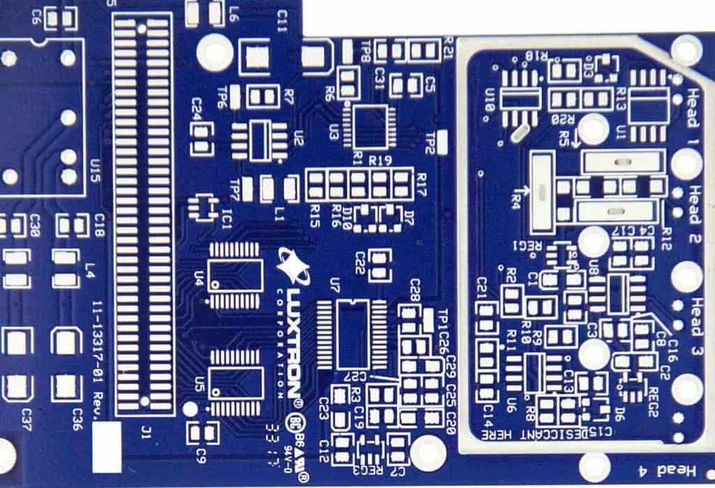
Immersion tin, often abbreviated as ImSn, is a surface finish applied to PCBs through a chemical displacement process. Unlike other finishes that use electroplating, immersion tin relies on a chemical reaction where tin ions in a solution replace copper atoms on the PCB surface, forming a thin, uniform layer of tin. This layer typically ranges from 0.8 to 1.2 micrometers in thickness, providing a protective barrier against oxidation while maintaining a flat surface for soldering.
This finish is widely used in the electronics industry due to its simplicity and compatibility with lead-free soldering processes. It’s particularly favored in applications requiring fine-pitch components because of its smooth and even coating. However, as we’ll discuss later, immersion tin has specific challenges that may affect its suitability for certain projects.
Advantages of Immersion Tin PCB Finish
When considering immersion tin advantages, several key benefits stand out for engineers and manufacturers looking for a reliable surface finish. Below, we break down the primary reasons why immersion tin is a popular choice.
1. Excellent Solderability
One of the standout features of immersion tin solderability is its ability to provide a clean, oxide-free surface for soldering. The tin layer prevents copper oxidation, ensuring strong and reliable solder joints. This makes it ideal for lead-free soldering processes, which are common in modern electronics due to environmental regulations. Tests have shown that immersion tin maintains its solderability even after multiple reflow cycles, with wetting times often below 1 second under standard conditions (e.g., 260°C for lead-free solder).
2. Cost-Effective Solution
Immersion tin cost is another major advantage. Compared to other surface finishes like ENIG (Electroless Nickel Immersion Gold), immersion tin is generally less expensive to apply. The process doesn’t require complex equipment or costly materials like gold, making it a budget-friendly option for high-volume production. For instance, while ENIG might cost 20-30% more per square inch, immersion tin offers a more economical alternative without sacrificing essential performance in many cases.
3. Flat and Uniform Surface
The immersion tin process creates a very flat and consistent coating, which is critical for fine-pitch components and surface-mount technology (SMT). Uneven surfaces can lead to soldering defects, but immersion tin’s uniformity—often with thickness variations of less than 0.1 micrometers—ensures precise placement and reliable connections. This is especially beneficial for high-density PCB designs where component spacing is tight.
4. Environmentally Friendly
Immersion tin is a lead-free and RoHS-compliant finish, aligning with global environmental standards. It avoids hazardous substances like lead or cadmium, making it a safer choice for both manufacturers and end-users. This compliance is crucial for industries targeting markets with strict environmental regulations.
Disadvantages of Immersion Tin PCB Finish
While immersion tin offers many benefits, it’s not without its challenges. Understanding the immersion tin disadvantages is essential for determining whether this finish suits your specific needs.
1. Limited Shelf Life
One of the most significant drawbacks of immersion tin is its relatively short shelf life. Over time, the tin layer can form intermetallic compounds with the underlying copper, leading to a phenomenon known as “tin whiskers.” These microscopic growths can cause short circuits in high-density designs. Typically, immersion tin PCBs are best used within 6-12 months of manufacturing to avoid degradation in solderability.
2. Sensitivity to Handling
The tin layer is soft and prone to scratching or damage during handling. Even minor abrasions can expose the underlying copper, leading to oxidation and soldering issues. Manufacturers often need to implement strict handling protocols or use protective packaging to prevent surface damage, adding to production complexity.
3. Not Ideal for Multiple Reflows
Although immersion tin provides good solderability initially, its performance can degrade after multiple reflow cycles. The thin tin layer may fully convert to intermetallic compounds during repeated heating, reducing the available tin for soldering. For projects requiring multiple assembly stages, other finishes like ENIG might be more suitable.
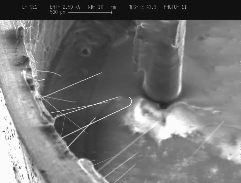
4. Risk of Tin Whiskers
As mentioned earlier, tin whiskers are a notable concern with immersion tin. These tiny, hair-like structures can grow over time, especially under conditions of mechanical stress or high humidity. While the risk is lower with modern formulations (often incorporating additives to mitigate whisker growth), it remains a potential issue for critical applications like aerospace or medical devices.
Immersion Tin Applications: Where Does It Shine?
Immersion tin applications span various industries and use cases, thanks to its balance of cost and performance. Below are some common scenarios where this finish excels.
1. Consumer Electronics
Immersion tin is widely used in consumer electronics like smartphones, tablets, and wearables. Its flat surface supports the fine-pitch components common in these devices, while its cost-effectiveness suits high-volume production. For example, many budget-friendly gadgets rely on immersion tin to keep manufacturing expenses low without compromising basic reliability.
2. Automotive Electronics
In automotive applications, immersion tin is often chosen for non-critical components like infotainment systems or interior controls. Its lead-free nature aligns with industry regulations, and its solderability ensures dependable connections in less demanding environments. However, for high-reliability parts exposed to extreme conditions, other finishes may be preferred.
3. Industrial Control Systems
For industrial PCBs used in control systems or sensors, immersion tin provides a practical solution. These applications often prioritize cost and ease of assembly over long-term durability, making immersion tin a fitting choice. Its uniform coating also supports automated soldering processes commonly used in industrial manufacturing.
4. Prototyping and Short-Run Production
Immersion tin is a go-to option for prototyping or short-run PCB production. Its lower cost compared to premium finishes allows designers to test designs without breaking the budget. Since prototypes are often assembled and tested within a short timeframe, the limited shelf life of immersion tin is rarely an issue in these scenarios.
Immersion Tin vs ENIG: A Detailed Comparison
When choosing a PCB surface finish, one common comparison is immersion tin vs ENIG. Both have their strengths and weaknesses, and the right choice depends on your project’s specific requirements. Let’s break down the key differences across several factors.
1. Solderability
Both immersion tin and ENIG offer excellent solderability, but they behave differently over time. Immersion tin provides a clean soldering surface initially but can degrade after 6-12 months due to intermetallic formation. ENIG, with its gold top layer over nickel, maintains solderability for longer periods, often exceeding 12-18 months, even under challenging storage conditions.
2. Cost
Immersion tin cost is significantly lower than ENIG. The absence of gold and nickel layers reduces material and processing expenses, making immersion tin 20-30% cheaper on average. For budget-conscious projects or high-volume runs, immersion tin often wins out. ENIG, however, justifies its higher cost with superior durability and performance in demanding applications.
3. Durability and Shelf Life
ENIG outperforms immersion tin in terms of durability. The gold layer in ENIG is highly resistant to oxidation and handling damage, while the nickel underlayer prevents copper diffusion. This makes ENIG ideal for long-term storage and harsh environments. Immersion tin, as noted earlier, has a shorter shelf life and is more susceptible to surface damage.
4. Applications Suitability
Immersion tin suits cost-sensitive, short-term, or less critical applications like consumer electronics and prototyping. ENIG is preferred for high-reliability uses, such as medical devices, aerospace systems, and telecommunications equipment, where long-term performance and resistance to environmental factors are crucial.
Immersion Tin Solderability: What You Need to Know
Immersion tin solderability is one of its strongest selling points, especially for lead-free assembly processes. The tin layer ensures a clean, oxide-free surface that readily accepts solder, resulting in strong joints. Wetting balance tests often show immersion tin achieving full wetting in under 1 second at 260°C, which is comparable to more expensive finishes in initial performance.
However, solderability diminishes over time due to the formation of copper-tin intermetallic compounds. To maximize performance, it’s recommended to assemble immersion tin PCBs within 6 months of fabrication. Proper storage—keeping boards in a dry, temperature-controlled environment—can also help preserve solderability. For applications requiring multiple reflows, consider limiting the number of heat cycles to 2-3 to avoid depleting the tin layer.
Immersion Tin Cost: Budget-Friendly but with Trade-Offs
The immersion tin cost is a major reason for its popularity, especially in cost-sensitive projects. On average, immersion tin is priced at approximately $0.05 to $0.10 per square inch for standard PCB sizes, though this can vary based on volume and supplier. Compared to ENIG, which can range from $0.07 to $0.15 per square inch, immersion tin offers significant savings, particularly for large-scale production.
However, the lower upfront cost comes with trade-offs like shorter shelf life and potential rework expenses if solderability issues arise. When budgeting for your project, weigh these factors against the initial savings to determine if immersion tin is the most economical choice in the long run.
Tips for Working with Immersion Tin PCB Finish
To get the most out of immersion tin, follow these practical tips during design, manufacturing, and assembly:
- Plan for Quick Assembly: Schedule assembly within 6-12 months of PCB fabrication to avoid solderability issues.
- Handle with Care: Use gloves and protective packaging to prevent scratches or contamination of the tin surface.
- Store Properly: Keep PCBs in a cool, dry place with humidity below 50% to minimize oxidation and tin whisker growth.
- Limit Reflow Cycles: Design your assembly process to minimize heat exposure, ideally keeping reflow cycles under 3.
- Test for Compatibility: If using immersion tin for fine-pitch components, conduct soldering tests to ensure consistent results.
Conclusion: Is Immersion Tin Right for Your Project?
Immersion tin PCB finish offers a compelling mix of affordability, solderability, and compatibility with modern manufacturing needs. Its advantages, such as low cost and a flat surface for fine-pitch components, make it a go-to choice for consumer electronics, prototyping, and other cost-sensitive applications. However, its disadvantages—limited shelf life, sensitivity to handling, and risk of tin whiskers—mean it’s not always the best fit for high-reliability or long-term projects.
When comparing immersion tin vs ENIG, consider your project’s priorities. If budget and short-term performance are key, immersion tin is an excellent option. For applications demanding durability and extended shelf life, a premium finish like ENIG might be worth the added cost. By understanding the strengths and limitations of immersion tin, you can make a confident decision that aligns with your design goals and production timeline.
At ALLPCB, we’re committed to helping you choose the right surface finish for your PCBs. Whether it’s immersion tin or another option, our expertise ensures your boards meet the highest standards of quality and performance. Explore our services to bring your next project to life with precision and efficiency.


