 ALLPCB


Are you wondering about the smallest functional PCB size possible for your next project? The answer depends on various factors, including design rules, component sizes, and manufacturing capabilities. In general, functional PCBs can be as small as a few millimeters in dimensions—think 5mm x 5mm or even smaller for highly specialized applications like medical implants or IoT devices. However, achieving such tiny sizes comes with significant challenges in design, fabrication, and assembly.
In this detailed guide, we'll dive deep into the world of PCB miniaturization, exploring the smallest PCB dimensions, minimum PCB area, functional PCB size limits, and the hurdles of micro PCB design rules. Whether you're an engineer working on compact electronics or a designer pushing the boundaries of innovation, this post will provide valuable insights to help you navigate the complexities of creating tiny yet functional circuit boards.
Understanding PCB Miniaturization: Why Size Matters
In today's fast-paced tech world, smaller is often better. From wearable gadgets to smart sensors, the demand for compact electronics continues to drive PCB miniaturization. Reducing the size of a printed circuit board (PCB) not only saves space but also cuts down on material costs and power consumption, making devices more efficient.
However, shrinking a PCB to the smallest possible dimensions isn't just about making it fit into a tiny enclosure. It involves balancing functionality, reliability, and manufacturability. As we push toward smaller designs, we encounter limitations in component placement, trace widths, and even heat dissipation. Let's explore what defines the smallest functional PCB size and the factors that influence it.
What Are the Smallest PCB Dimensions Achievable Today?
The smallest functional PCB dimensions depend heavily on the technology and tools available during manufacturing. For most commercial applications, PCBs as small as 5mm x 5mm are achievable with standard surface-mount technology (SMT). However, in specialized fields like medical devices or aerospace, boards can shrink to even smaller sizes, sometimes down to 2mm x 2mm or less.
For context, some microcontrollers now come in wafer chip-scale packages (WCSP) measuring just 1.38mm2 in area. These tiny chips are often paired with equally small PCBs to create ultra-compact systems. But while the theoretical minimum PCB area might seem limitless, practical constraints like component footprints, soldering requirements, and signal integrity set real-world boundaries.
In high-density designs, micro vias (as small as 0.1mm in diameter) and trace widths of 0.075mm (3 mils) are often used to pack more functionality into a tiny space. These specs are within the capabilities of advanced PCB fabrication processes, but they require precision and expertise to execute without errors.
Functional PCB Size Limits: What's the Bare Minimum?
Determining the functional PCB size limits involves understanding the minimum area needed to support the required components and connections. At a basic level, a functional PCB must accommodate:
- The smallest components, such as 0201 or 01005 SMD (surface-mount device) resistors and capacitors, which measure just 0.6mm x 0.3mm or 0.4mm x 0.2mm, respectively.
- Enough space for traces and vias to ensure proper electrical connections without interference.
- Sufficient area for soldering pads, even if using automated assembly with micro-scale precision.
For a simple circuit with a single microcontroller and a few passive components, a PCB as small as 3mm x 3mm might be functional. However, this assumes the use of advanced assembly techniques and high-density interconnect (HDI) technology. For more complex designs, the minimum area increases to accommodate additional layers, larger components, or specific routing needs.
PCB Miniaturization Challenges: Why Smaller Isn’t Always Easier
While the idea of shrinking a PCB to the smallest possible size is exciting, it comes with a host of challenges. Miniaturization pushes the limits of design and manufacturing, often leading to trade-offs in performance or cost. Here are some of the key PCB miniaturization challenges to consider:
1. Component Density and Placement
As PCBs get smaller, fitting all necessary components into a limited space becomes tricky. High component density can lead to issues like crosstalk, where signals from adjacent traces interfere with each other. For instance, maintaining a signal integrity of 50 ohms impedance in high-speed designs requires careful spacing, which is harder in micro PCBs.
2. Thermal Management
Smaller PCBs have less surface area to dissipate heat. Without proper thermal vias or heat sinks, components can overheat, reducing lifespan or causing failures. For example, a power-intensive chip on a 5mm x 5mm board might reach temperatures exceeding 85°C without adequate cooling, risking damage.
3. Manufacturing Precision
Fabricating micro PCBs requires extreme precision. Trace widths below 0.1mm and via diameters under 0.15mm demand advanced equipment and strict quality control. Even a slight misalignment during assembly can result in short circuits or broken connections.
4. Signal Integrity and Noise
In tiny PCBs, traces are closer together, increasing the risk of electromagnetic interference (EMI). High-speed signals, such as those running at 1 GHz or more, are particularly vulnerable to noise and require careful routing and shielding, which is challenging in a confined space.
Micro PCB Design Rules: Guidelines for Success
Designing a micro PCB that functions reliably at the smallest possible size requires adherence to strict design rules. These micro PCB design rules help ensure manufacturability and performance, even when working with minimal dimensions. Below are some essential guidelines to follow:
1. Optimize Component Selection
Choose the smallest components available for your design. Opt for chip-scale packages (CSP) or ball grid arrays (BGA) with fine pitches (as low as 0.4mm) to save space. Always check the footprint requirements and ensure they align with your PCB’s dimensions.
2. Use High-Density Interconnect (HDI) Technology
HDI PCBs allow for finer traces, smaller vias, and more layers in a compact area. This technology is crucial for achieving minimum PCB areas while maintaining functionality. For instance, micro vias with diameters of 0.1mm enable tighter routing in multi-layer designs.
3. Minimize Trace Widths and Spacing
Follow the smallest trace widths and spacing your manufacturer can reliably produce. Many advanced fabrication processes support traces as narrow as 0.075mm (3 mils) with matching spacing. However, ensure these values don’t compromise signal integrity or current-carrying capacity.
4. Plan for Multi-Layer Designs
When surface area is limited, stacking layers vertically is often the solution. A 4-layer or 6-layer PCB can pack more circuitry into a small footprint, though it increases fabrication complexity and cost. Use blind and buried vias to connect layers without wasting space.
5. Test for Signal and Power Integrity
Simulate your design to check for potential issues like voltage drops or signal delays. For high-speed circuits, ensure impedance matching (e.g., 50 ohms for RF signals) and avoid sharp bends in traces that could cause reflections.
Applications of the Smallest Functional PCBs
The drive toward smaller PCB sizes has opened up exciting possibilities across various industries. Here are some real-world applications where the smallest functional PCB dimensions are making a big impact:
- Medical Devices: Implantable devices like pacemakers and hearing aids rely on micro PCBs measuring just a few millimeters to fit inside the human body while delivering life-saving functionality.
- IoT Sensors: Smart sensors for environmental monitoring or home automation often use tiny PCBs to remain unobtrusive while collecting and transmitting data.
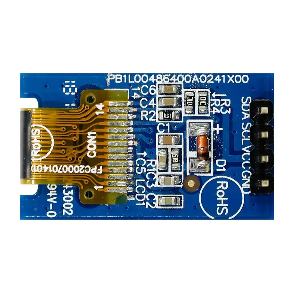
- Wearable Technology: Smartwatches and fitness trackers pack powerful electronics into wrist-sized devices, often with PCBs smaller than 10mm x 10mm.
- Aerospace: Satellites and drones use compact PCBs to save weight and space, ensuring efficient operation in harsh environments.
How to Achieve the Smallest Functional PCB Size for Your Project
If you're aiming to design a PCB with the smallest possible dimensions, follow these actionable steps to ensure success:
- Define Your Requirements: Start by listing the components and functionality your PCB must support. This helps determine the minimum area needed.
- Collaborate with Manufacturers: Work closely with your PCB fabrication and assembly partners to understand their capabilities, such as minimum trace widths or via sizes.
- Use Design Software: Leverage advanced PCB design tools to simulate layouts, optimize spacing, and identify potential issues before fabrication.
- Iterate and Test: Build prototypes of your micro PCB and test them under real-world conditions to ensure reliability and performance.
Conclusion: Pushing the Boundaries of PCB Miniaturization
The smallest functional PCB size is no longer just a theoretical concept—it's a reality in industries ranging from healthcare to consumer electronics. While PCBs as small as 2mm x 2mm or even less are possible with cutting-edge technology, achieving these dimensions requires overcoming significant PCB miniaturization challenges. By following micro PCB design rules, optimizing component selection, and leveraging advanced manufacturing techniques, engineers can push the boundaries of what's possible.


