 ALLPCB


If you're looking to enhance power integrity in your PCB designs, stacked vias for Power Distribution Networks (PDN) are a game-changer. They help achieve low impedance, ensuring stable power delivery to critical components. In this comprehensive guide, we'll dive deep into how stacked vias work in PDN, why they matter for power distribution, and how to optimize them for the best results in PCB design. Whether you're tackling high-speed circuits or complex multilayer boards, this blog will equip you with actionable insights to improve power integrity.
What Are Stacked Vias and Why Are They Important for PDN?
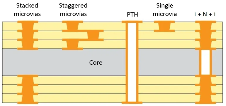
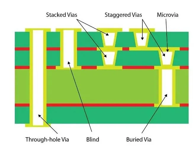
Stacked vias are vertical interconnects in a printed circuit board (PCB) that connect multiple layers directly on top of each other, unlike staggered vias which are offset. In the context of Power Distribution Networks (PDN), stacked vias play a crucial role by providing a direct, low-impedance path for power and ground connections between layers. This ensures that power is delivered efficiently to components without significant voltage drops or noise.
Power integrity is a top concern in modern PCB design, especially for high-speed and high-performance applications. A well-designed PDN minimizes impedance, reduces noise, and prevents issues like signal distortion or system failures. Stacked vias help achieve this by shortening the current path and reducing parasitic inductance, which can otherwise disrupt power delivery. For instance, in a multilayer PCB, using stacked vias can lower loop inductance by up to 30% compared to staggered vias, ensuring cleaner power distribution.
The Role of Low Impedance in Power Distribution
Low impedance is the backbone of an effective PDN. Impedance in a power distribution network refers to the opposition to current flow, and high impedance can lead to voltage drops, noise, and poor performance in high-speed circuits. Stacked vias are a key strategy for achieving low impedance because they create a more direct connection between power and ground planes, minimizing the path length that current must travel.
In practical terms, reducing impedance can mean the difference between a stable system and one plagued by power integrity issues. For example, in a high-speed design operating at 1 GHz, even a small inductance of 1 nH can cause significant noise. Stacked vias can cut this inductance down by providing a shorter, more efficient path, often reducing impedance by 20-40% compared to traditional via arrangements.
By focusing on low impedance in your PDN, you ensure that components receive the stable voltage they need, even under dynamic load conditions. This is especially critical for applications like data centers, telecommunications, and automotive electronics, where power demands fluctuate rapidly.
Advantages of Stacked Vias in PCB Design for Power Integrity
Using stacked vias in your PCB design offers several benefits that directly impact power integrity and overall board performance. Let's break down the key advantages:
- Reduced Parasitic Inductance: Stacked vias minimize the loop area for current flow, cutting down on parasitic inductance. This is vital for high-frequency designs where even small inductance can introduce noise.
- Improved Power Delivery: With a shorter path between power and ground planes, stacked vias ensure faster and more efficient power delivery, reducing voltage drops.
- Space Efficiency: Stacked vias take up less horizontal space compared to staggered vias, allowing for denser layouts in multilayer boards.
- Enhanced Signal Integrity: By stabilizing the power supply, stacked vias indirectly improve signal integrity, as components receive consistent voltage without fluctuations.
These benefits make stacked vias a preferred choice for engineers working on complex designs where power integrity cannot be compromised. For instance, in a 10-layer PCB for a server application, using stacked vias can help maintain a target impedance of below 1 mΩ across critical power nets, ensuring reliable operation.
Design Considerations for Stacked Vias in PDN
While stacked vias offer significant advantages, their implementation requires careful planning to avoid potential pitfalls. Here are some critical design considerations to keep in mind:
1. Manufacturing Constraints
Stacked vias, especially those involving microvias, can be more challenging and costly to manufacture compared to staggered vias. They often require advanced processes like sequential lamination or laser drilling. Ensure that your design aligns with the capabilities of your fabrication partner to avoid delays or defects. For example, microvias used in stacked configurations typically have a diameter of 0.1 mm to 0.15 mm, and not all manufacturers can reliably produce these small features.
2. Thermal Management
Stacked vias can concentrate heat in a small area due to high current density. To prevent overheating, consider adding thermal vias nearby or using thicker copper layers for power planes. A general rule of thumb is to maintain a current density below 500 A/cm2 to avoid thermal issues.
3. Placement and Routing
Place stacked vias strategically close to high-current components like processors or FPGAs to minimize the distance power must travel. Additionally, ensure that power and ground vias are paired closely to reduce loop inductance. A common practice is to place a ground via within 0.5 mm of each power via to optimize the current return path.
4. Layer Stackup Design
In multilayer PCBs, the arrangement of power and ground planes impacts PDN performance. Position power and ground planes adjacent to each other to maximize capacitance and reduce impedance. Stacked vias should connect directly through these planes without unnecessary detours to maintain low impedance.
Optimization Strategies for Stacked Via PDN
To get the most out of stacked vias in your PDN, optimization is key. Here are some proven strategies to enhance power distribution and maintain power integrity:
1. Use Decoupling Capacitors Effectively
Decoupling capacitors work hand-in-hand with stacked vias to stabilize voltage and filter noise. Place high-frequency capacitors (e.g., 0.1 μF) as close as possible to power pins of ICs, and connect them to power and ground planes using stacked vias. This setup can reduce impedance peaks at frequencies up to 100 MHz, ensuring a flatter impedance profile.
2. Minimize Via Count Without Sacrificing Performance
While it might be tempting to use many stacked vias for redundancy, too many vias can increase manufacturing complexity and cost. Use simulation tools to determine the optimal number of vias needed to meet your impedance targets. For example, in a design with a 1.2 V power rail, simulations might show that four stacked vias per power pin are sufficient to keep impedance below 5 mΩ.
3. Leverage Simulation and Analysis Tools
Power integrity simulation tools can model the behavior of your PDN and help identify potential issues before fabrication. These tools analyze factors like impedance, voltage drop, and current density, allowing you to fine-tune the placement and configuration of stacked vias. Aim for a target impedance that’s at least 10% below the maximum allowable value for your design to account for manufacturing variations.
4. Balance Cost and Performance
Stacked vias, especially those involving blind or buried microvias, can increase production costs. Weigh the performance benefits against budget constraints. For less demanding applications, a hybrid approach combining stacked and staggered vias might provide a cost-effective compromise while still maintaining adequate power integrity.
Common Challenges and How to Overcome Them
Designing a PDN with stacked vias isn’t without challenges. Here are some common issues engineers face and practical solutions to address them:
- Signal Crosstalk: Stacked vias placed too close to signal traces can cause crosstalk, degrading signal integrity. Maintain a clearance of at least 3x the via diameter between signal traces and power vias to minimize interference.
- Reliability Concerns: Repeated thermal cycles can stress stacked vias, especially microvias, leading to cracks or failures. Use high-quality materials with a low coefficient of thermal expansion (CTE) and adhere to industry standards like IPC-6012 for via reliability.
- High Current Handling: In designs with high current demands, a single stacked via may not suffice. Use multiple vias in parallel to distribute current evenly, ensuring each via handles no more than 1-2 A to prevent overheating.
Real-World Applications of Stacked Vias in PDN
Stacked vias are widely used in industries where power integrity is non-negotiable. In telecommunications equipment, for example, they ensure stable power delivery to high-speed transceivers operating at frequencies above 10 GHz. In automotive electronics, stacked vias help manage power distribution in advanced driver-assistance systems (ADAS), where reliability under varying thermal conditions is critical. Even in consumer electronics like smartphones, stacked vias enable compact, multilayer designs without sacrificing performance.
Consider a high-speed server board with a 12-layer stackup. By using stacked vias to connect power and ground planes directly beneath critical components, engineers can achieve a target impedance of 0.5 mΩ, ensuring that voltage fluctuations stay within ±5% of the nominal value, even under heavy load.
Conclusion: Elevating Power Integrity with Stacked Vias
Stacked vias are a powerful tool for optimizing Power Distribution Networks in PCB design. By reducing impedance, improving power delivery, and enhancing overall power integrity, they enable engineers to tackle the challenges of modern high-speed and high-performance applications. While their design and implementation require careful planning, the benefits of stacked vias far outweigh the complexities when executed correctly.
From strategic placement and layer stackup design to leveraging simulation tools and balancing cost, the key to success lies in thoughtful optimization. As PCB designs continue to push boundaries in terms of speed and density, mastering the use of stacked vias for PDN will remain a critical skill for engineers aiming to deliver reliable, efficient, and high-performing boards.
With the insights and strategies shared in this guide, you're well-equipped to integrate stacked vias into your next project and achieve a low-impedance, high-integrity power distribution network that meets the demands of even the most complex designs.


