 ALLPCB


When it comes to Ball Grid Array (BGA) assembly, one often overlooked but critical factor is the solder mask thickness. This thin layer of protective coating on a printed circuit board (PCB) can make or break the reliability of connections in high-density designs. For engineers and designers working on complex projects, understanding the impact of solder mask thickness for BGA, along with proper BGA pad design, is essential for ensuring a smooth assembly process and long-term performance. In this blog, we'll dive deep into why solder mask thickness matters, how it interacts with solder mask defined pads and non-solder mask defined pads, and best practices for the BGA assembly process.
Why Solder Mask Thickness Matters for BGA Assembly
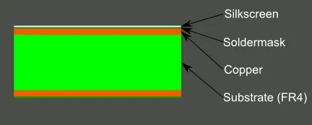
Solder mask is a thin polymer layer applied to a PCB to protect copper traces from oxidation and prevent unintended solder bridges during assembly. For BGA components, which feature a grid of tiny solder balls on the underside, the solder mask plays an even more crucial role. The thickness of this layer directly affects how well the solder balls connect to the PCB pads, impacting both mechanical stability and electrical performance.
In typical PCB designs, solder mask thickness ranges from 0.8 to 1.2 mils (20 to 30 micrometers). However, for BGA applications, even a slight variation in this range can lead to issues like insufficient solder joint formation or excessive mask interference. If the solder mask is too thick, it may encroach on the pad area, reducing the effective contact surface for the solder ball. If it’s too thin, it might not provide adequate protection, leading to shorts or contamination during the BGA assembly process.
Understanding Solder Mask Defined Pads vs. Non-Solder Mask Defined Pads
When designing pads for BGA components, one key decision is whether to use solder mask defined (SMD) pads or non-solder mask defined (NSMD) pads. Both approaches have unique implications for solder mask thickness and overall assembly reliability.
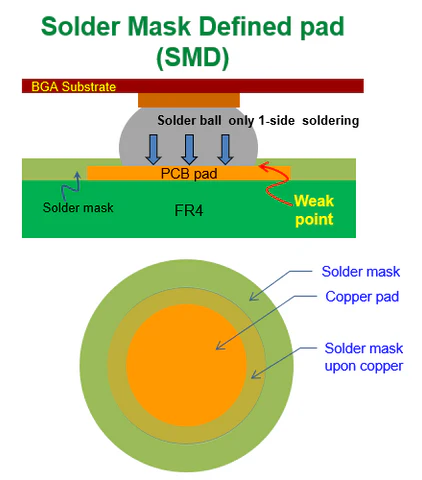
Solder Mask Defined Pads (SMD)
In SMD pad design, the solder mask overlaps the edges of the copper pad, defining the area where solder can adhere. This method is often used for finer pitch BGAs (where the distance between solder balls is less than 0.5 mm) because it provides better control over the solderable area. However, the solder mask thickness for BGA must be carefully managed with SMD pads. If the mask is too thick, it can create a "step" that interferes with the solder ball seating, leading to weak joints. A typical clearance of 2 to 3 mils (50 to 75 micrometers) between the mask edge and pad is recommended to avoid such issues.
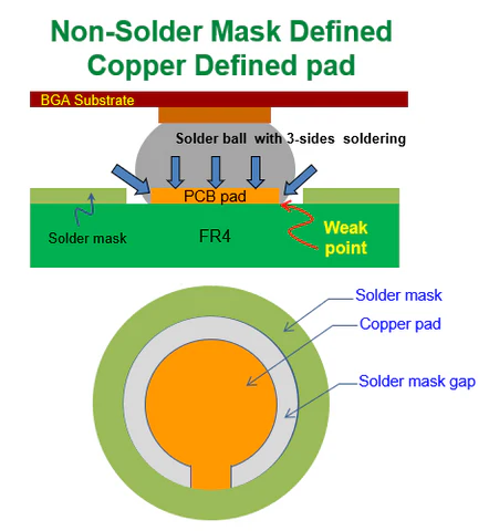
Non-Solder Mask Defined Pads (NSMD)
NSMD pads, on the other hand, have the solder mask pulled back from the copper pad, exposing the entire pad and sometimes a small portion of the surrounding trace. This design allows for a larger solderable area, which can improve the strength of the solder joint. For NSMD pads, solder mask thickness is less of a direct concern since the mask doesn’t encroach on the pad. However, maintaining a consistent thickness—typically around 0.8 to 1.0 mils (20 to 25 micrometers)—still ensures proper insulation and prevents solder bridging during the BGA assembly process.
For most modern BGA designs, NSMD pads are preferred due to their ability to form stronger, more reliable connections. Studies have shown that NSMD pads can improve solder joint reliability by up to 20% under thermal cycling tests compared to SMD pads, especially in high-density applications.
BGA Pad Design: Key Considerations for Optimal Performance
Beyond choosing between SMD and NSMD pads, BGA pad design requires attention to several factors to ensure reliable connections. These include pad size, pitch, and alignment with solder mask thickness for BGA applications.
Pad Size and Pitch
The pad size for BGA components should typically be 80-90% of the solder ball diameter to ensure proper wetting during reflow soldering. For example, a 0.5 mm diameter solder ball would pair well with a pad diameter of 0.4 to 0.45 mm. The pitch, or spacing between solder balls, also influences pad design. Fine-pitch BGAs (below 0.5 mm) often require tighter control over solder mask thickness to prevent bridging, while larger pitches (0.8 mm and above) are more forgiving.
Solder Mask Expansion
Solder mask expansion refers to the distance between the edge of the pad and the edge of the solder mask opening. For NSMD pads, an expansion of 2 to 4 mils (50 to 100 micrometers) is standard to allow for manufacturing tolerances and ensure the entire pad is exposed. Proper expansion also helps mitigate misregistration issues during PCB fabrication, which can be catastrophic for BGA assembly if the solder mask covers part of the pad.
Thermal and Electrical Considerations
BGA pad design must also account for thermal dissipation and signal integrity. For high-power BGAs, incorporating thermal vias beneath the pads can help dissipate heat, but these vias must be tented or filled to prevent solder wicking. Additionally, maintaining consistent solder mask thickness helps control impedance in high-speed designs. A thicker mask (around 1.2 mils or 30 micrometers) can slightly increase capacitance, which may be beneficial for reducing noise in high-frequency signals traveling at speeds above 1 GHz.
The BGA Assembly Process: How Solder Mask Thickness Impacts Each Step
The BGA assembly process involves several stages, from solder paste application to reflow soldering and inspection. At each step, solder mask thickness for BGA plays a subtle but significant role in ensuring success.
Solder Paste Application
During solder paste printing, the solder mask acts as a stencil guide to ensure paste is deposited only on the pads. If the solder mask thickness is uneven or too thick (exceeding 1.5 mils or 38 micrometers), it can cause inconsistent paste deposition, leading to voids or insufficient solder volume for the BGA balls. A uniform thickness of 0.8 to 1.2 mils (20 to 30 micrometers) is ideal for maintaining precision during this step.
Component Placement
Accurate placement of the BGA component is critical, and the solder mask helps by providing visual cues for alignment. For SMD pads, the mask’s edge defines the pad boundary, so any variation in thickness or misregistration can mislead automated placement machines. NSMD pads offer more flexibility since the entire pad is exposed, but the solder mask must still be consistent to avoid interference with the component’s seating.
Reflow Soldering
In the reflow soldering stage, the solder balls melt and bond with the pads. A solder mask that’s too thick can create a barrier, preventing proper wetting and leading to weak joints. Conversely, a mask that’s too thin may fail to prevent solder from spreading beyond the pad, risking shorts. Maintaining the recommended thickness ensures the solder flows evenly, forming reliable connections with shear strength values often exceeding 5 kg for standard 0.5 mm pitch BGAs.
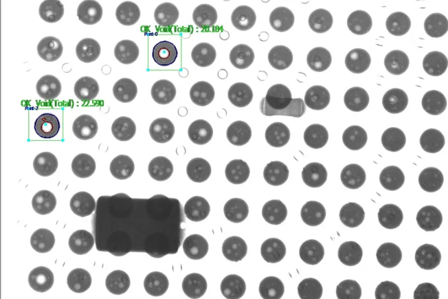
Inspection and Testing
After assembly, BGAs are inspected using X-ray systems to check for voids, misalignments, or insufficient solder joints. A well-controlled solder mask thickness minimizes these defects, reducing the need for rework. For instance, a solder mask thickness deviation of just 0.2 mils (5 micrometers) can increase voiding rates by up to 10%, according to industry studies, highlighting the importance of precision.
Best Practices for Managing Solder Mask Thickness in BGA Designs
To achieve reliable connections in BGA assembly, follow these actionable best practices for managing solder mask thickness and related design elements.
- Specify Thickness in Fabrication Notes: Clearly communicate the desired solder mask thickness (e.g., 0.8 to 1.2 mils or 20 to 30 micrometers) in your PCB design files to avoid manufacturing errors.
- Choose NSMD for Most Applications: Unless fine-pitch constraints dictate otherwise, opt for non-solder mask defined pads to maximize solderable area and improve joint reliability.
- Control Solder Mask Expansion: Set an expansion value of 2 to 4 mils (50 to 100 micrometers) for NSMD pads to account for fabrication tolerances.
- Collaborate with Fabricators: Work closely with your PCB manufacturer to ensure consistent application of solder mask, especially for high-density BGA layouts.
- Test Under Real Conditions: Perform thermal cycling and mechanical stress tests on prototypes to verify that solder mask thickness and pad design withstand operational demands.
Common Challenges and How to Overcome Them
Even with careful planning, challenges related to solder mask thickness for BGA can arise. Here are some common issues and solutions.
Misregistration of Solder Mask
Misregistration occurs when the solder mask layer isn’t perfectly aligned with the pads, potentially covering part of the solderable area. This is more problematic for SMD pads. To mitigate this, use a slightly larger solder mask expansion and request tight registration tolerances (e.g., ±2 mils or ±50 micrometers) during fabrication.
Solder Bridging
For fine-pitch BGAs, solder bridging between pads is a risk if the solder mask is too thin or poorly applied. Ensure the mask thickness is at least 0.8 mils (20 micrometers) and consider using high-quality liquid photoimageable (LPI) solder mask materials for better definition.
Thermal Stress Failures
During operation, BGAs are subjected to thermal expansion and contraction, which can stress solder joints. A consistent solder mask thickness helps maintain pad integrity, while NSMD designs distribute stress more evenly across the joint, reducing failure rates by up to 15% in some thermal cycling tests.
Conclusion: Precision in Solder Mask Thickness for BGA Success
In the world of high-density PCB design, every detail counts, and solder mask thickness for BGA assembly is no exception. By carefully managing this parameter, along with thoughtful BGA pad design using solder mask defined or non-solder mask defined pads, engineers can ensure reliable connections throughout the BGA assembly process. Whether you’re dealing with fine-pitch components or high-power applications, adhering to best practices for solder mask thickness—typically 0.8 to 1.2 mils (20 to 30 micrometers)—and collaborating with your manufacturer will lead to better outcomes. With the right approach, you can minimize defects, enhance performance, and build PCBs that stand the test of time.


