ALLPCB


If you're a PCB designer looking for a clear understanding of prepreg thickness, you're in the right place. Prepreg, a critical material in printed circuit board (PCB) manufacturing, directly impacts the performance, durability, and reliability of your designs. In this guide, we'll cover everything you need to know about PCB prepreg thickness, including how to select the right material, design effective stackups, understand tolerances, and explore different prepreg types. Let's dive into this essential topic to help you create better PCBs with confidence.
What Is Prepreg and Why Does Thickness Matter?
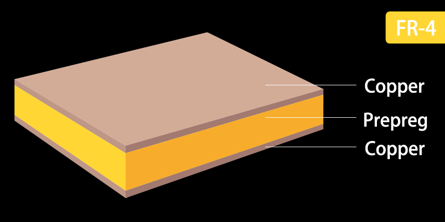
Prepreg, short for "pre-impregnated," is a fiberglass fabric soaked with resin (usually epoxy) and partially cured to a semi-solid state. It acts as an insulating layer and adhesive between copper layers in a multilayer PCB. During the lamination process, prepreg melts and bonds the layers together under heat and pressure, forming a solid structure.
The thickness of prepreg is crucial because it affects several key aspects of a PCB:
- Dielectric Properties: Prepreg thickness influences impedance control, which is vital for high-speed signal integrity. For example, a thinner prepreg layer can reduce the dielectric spacing between signal and ground planes, affecting characteristic impedance (often targeted at 50 ohms for many designs).
- Mechanical Strength: Proper thickness ensures the PCB can withstand physical stress during assembly and operation.
- Thermal Performance: Thickness impacts heat dissipation, especially in high-power applications.
- Overall Board Thickness: Prepreg layers contribute to the final thickness of the PCB, which must meet design specifications (commonly 1.6mm for standard boards).
Understanding and selecting the right prepreg thickness is a foundational step in PCB stackup design. Let's explore this in detail to ensure your designs meet both electrical and mechanical requirements.
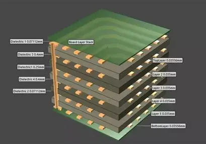
Understanding Prepreg Thickness in PCB Stackup Design
PCB stackup design refers to the arrangement of copper layers and insulating materials (like prepreg and core) in a multilayer board. Prepreg thickness plays a pivotal role in determining the spacing between conductive layers, which directly affects signal performance and manufacturing feasibility.
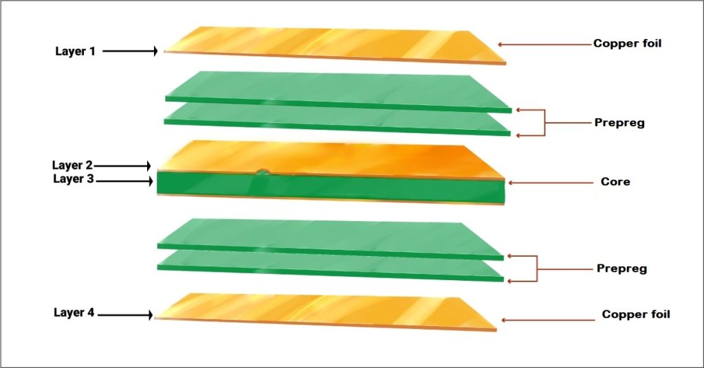
In a typical 4-layer PCB stackup, you might have:
- Top copper layer (signal)
- Prepreg (insulating layer)
- Inner copper layer (ground)
- Core (thicker insulating material)
- Inner copper layer (power)
- Prepreg (insulating layer)
- Bottom copper layer (signal)
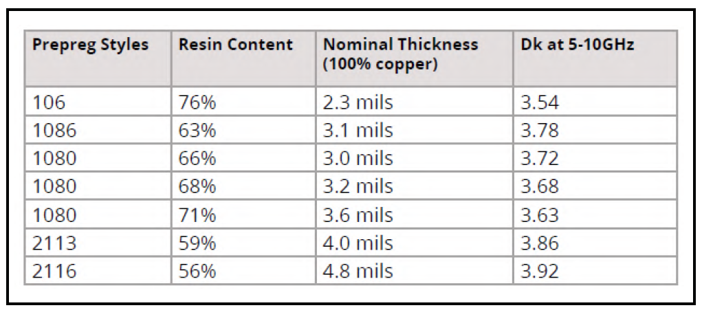
Prepreg thickness often ranges from 0.002 inches (2 mils) to 0.010 inches (10 mils) per layer, depending on the design needs. For high-speed designs, thinner prepreg layers (around 3-5 mils) are often used between signal and ground planes to maintain tight impedance control, typically targeting a dielectric constant (Dk) of around 4.0 for standard FR-4 materials.
Choosing the right prepreg thickness for your stackup involves balancing electrical performance with manufacturability. Thinner layers improve signal integrity but can increase manufacturing costs and complexity. Thicker layers are easier to handle but may not meet the tight tolerances needed for high-frequency applications.
How to Select the Right Prepreg Material and Thickness
Selecting the appropriate prepreg material and thickness is a critical decision in PCB design. Here are the key factors to consider when making your choice:
1. Electrical Requirements
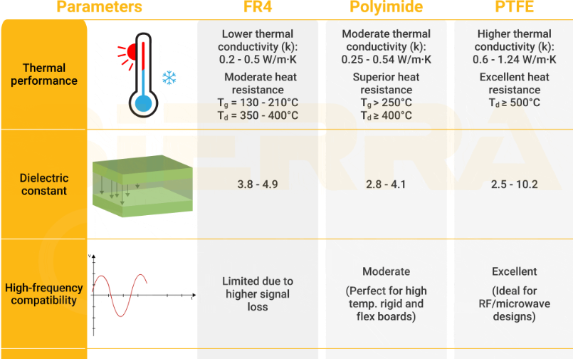
For high-speed or high-frequency designs, you need materials with low dielectric constants (Dk) and low loss tangents (Df) to minimize signal loss. Standard FR-4 prepreg has a Dk of about 4.0-4.5, while advanced materials like polyimide or PTFE-based prepregs can offer Dk values as low as 2.2 for better performance at frequencies above 1 GHz. Thinner prepreg layers are often preferred in these cases to maintain precise impedance, such as 50 ohms for single-ended traces.
2. Mechanical Constraints
The overall thickness of the PCB must fit within the mechanical constraints of the final product. If your design requires a total board thickness of 1.6mm, you’ll need to calculate the contribution of each prepreg layer alongside the core and copper thicknesses. A common prepreg thickness for standard designs is around 6-8 mils per layer.
3. Thermal Management
In applications with high power dissipation, thicker prepreg layers may help with thermal insulation between layers, preventing heat buildup. However, for better heat transfer, you might opt for thinner layers combined with thermal vias.
4. Cost and Availability
Thinner prepreg materials and specialty resins (like high-Tg or low-Dk options) often come at a higher cost. Balancing performance with budget constraints is essential, especially for mass production.
By aligning prepreg selection with your design goals—whether it’s signal integrity, thermal stability, or cost efficiency—you can optimize your PCB performance. Always consult with your manufacturing partner to ensure the chosen materials and thicknesses are compatible with their processes.
Prepreg Thickness Tolerances: What You Need to Know
Prepreg thickness tolerances refer to the acceptable variation in thickness during manufacturing. These tolerances are important because even small deviations can affect impedance, signal integrity, and the overall fit of the PCB in its enclosure.
For standard FR-4 prepreg, manufacturers often specify a tolerance of ±10% of the nominal thickness. For example, a 6-mil prepreg layer might vary between 5.4 mils and 6.6 mils. However, during the lamination process, factors like pressure, temperature, and resin flow can cause further variations, sometimes resulting in a final thickness tolerance of ±0.15mm for a 1.6mm board.
For high-precision designs, such as those in RF or high-speed digital applications, tighter tolerances are often required. In these cases, you might need to specify prepreg with a tolerance of ±5% or work with advanced materials that offer more consistent thickness control. Be aware that tighter tolerances can increase manufacturing costs, so plan accordingly.
To manage tolerances effectively:
- Include detailed stackup specifications in your design files, noting acceptable thickness ranges for each layer.
- Simulate impedance values using tools to predict how thickness variations might impact signal performance. For instance, a 10% variation in a 4-mil prepreg layer could shift impedance by 2-3 ohms, potentially causing signal mismatches.
- Collaborate with your manufacturer to confirm their capability to meet your tolerance requirements.
Understanding and accounting for prepreg thickness tolerances ensures your PCB performs as intended, even with minor manufacturing variations.
Types of Prepreg for PCB Designers
Prepreg comes in various types, each suited to different applications. Familiarizing yourself with these options will help you make informed decisions for your designs. Here are the most common prepreg types:
1. Standard FR-4 Prepreg
This is the most widely used prepreg material due to its balance of cost and performance. It has a glass transition temperature (Tg) of around 130-140°C and a Dk of 4.0-4.5. It’s ideal for general-purpose applications like consumer electronics. Common thicknesses range from 3 to 10 mils.
2. High-Tg Prepreg
With a Tg of 170-180°C or higher, high-Tg prepreg offers better thermal stability for applications exposed to elevated temperatures, such as automotive or industrial electronics. It’s slightly more expensive but worth it for reliability in harsh environments.
3. Low-Dk/Low-Df Prepreg
Designed for high-frequency and high-speed designs, these prepregs minimize signal loss and distortion. They often have a Dk below 3.5 and are used in RF, microwave, and 5G applications. Thicknesses are typically kept thin (2-5 mils) for tight impedance control.
4. Halogen-Free Prepreg
For environmentally friendly designs, halogen-free prepreg avoids the use of harmful chemicals. It’s often used in consumer products to comply with RoHS standards, though it may have slightly different mechanical properties compared to standard FR-4.
5. Flexible Prepreg
Used in flexible or rigid-flex PCBs, this type of prepreg is designed to bend without breaking. It’s commonly made from polyimide materials and used in wearable devices or compact electronics.
Each prepreg type serves a specific purpose, so choose based on your project’s electrical, thermal, and mechanical needs. Combining different prepreg types in a single stackup (hybrid stackup) is also possible for advanced designs requiring varied properties across layers.
Best Practices for Designing with Prepreg Thickness in Mind
To achieve optimal results in your PCB designs, follow these practical tips when working with prepreg thickness:
- Simulate Early: Use PCB design software to simulate stackup configurations and predict impedance based on prepreg thickness. For example, a 5-mil prepreg layer between a signal trace and ground plane might yield a 50-ohm impedance with a trace width of 6 mils on FR-4.
- Account for Resin Flow: During lamination, resin can flow and slightly alter prepreg thickness. Work with your manufacturer to understand their process and adjust your design if needed.
- Standardize Where Possible: Stick to commonly available prepreg thicknesses (like 4, 6, or 8 mils) to reduce costs and lead times, unless your design demands custom specifications.
- Consider Layer Count: More layers mean more prepreg, increasing overall thickness. Plan your stackup to avoid exceeding mechanical constraints.
- Test Prototypes: Build and test prototypes to verify that prepreg thickness and material choices meet performance expectations, especially for critical applications.
By incorporating these practices into your workflow, you can avoid common pitfalls and ensure your PCB design is both functional and manufacturable.
Common Challenges with Prepreg Thickness and How to Overcome Them
Even with careful planning, challenges related to prepreg thickness can arise. Here are a few common issues and solutions:
- Impedance Mismatch: Variations in prepreg thickness can cause impedance deviations. Use controlled dielectric materials and specify tight tolerances to minimize this risk.
- Delamination: If prepreg layers are too thin or incompatible with other materials, delamination can occur during thermal cycling. Choose materials with matching coefficients of thermal expansion (CTE) and adequate resin content.
- Excessive Board Thickness: Multiple prepreg layers can add up, exceeding design limits. Optimize your stackup by using thinner prepreg or reducing layer count where possible.
Proactive communication with your manufacturing partner can help address these challenges early in the design phase, saving time and resources.
Conclusion: Mastering Prepreg Thickness for Better PCB Designs
Prepreg thickness is a fundamental aspect of PCB design that influences everything from signal integrity to mechanical durability. By understanding how to select the right prepreg material, design effective stackups, manage tolerances, and choose the appropriate prepreg type, you can create reliable and high-performing PCBs tailored to your specific needs.
Whether you're working on a simple 2-layer board or a complex high-speed multilayer design, paying attention to prepreg thickness will elevate the quality of your work. Use the insights and best practices shared in this guide as a starting point to refine your approach and achieve consistent results in every project.