 ALLPCB


In the fast-paced world of electronics, achieving optimal signal integrity in printed circuit boards (PCBs) is a top priority for engineers working on high-speed designs. One key technique to ensure this is precision PCB drilling, particularly through controlled depth drilling. This process directly impacts signal quality by addressing issues like via stubs and impedance mismatches. In this comprehensive guide, we’ll explore how controlled depth drilling enhances PCB performance, focusing on long-tail keywords like controlled depth drilling PCB signal integrity, back drilling PCB impedance control, PCB via stub removal, high-speed PCB design guidelines, and minimizing signal reflections PCB. Let’s dive into the details of mastering this critical manufacturing step for cutting-edge designs.
Why Controlled Depth Drilling Matters for Signal Integrity
Signal integrity is the foundation of reliable performance in high-speed PCBs. As data rates climb beyond 10 Gbps in modern applications, even small imperfections in a PCB can lead to signal degradation, crosstalk, or electromagnetic interference (EMI). Controlled depth drilling, often referred to as back drilling, is a specialized manufacturing process that removes unused portions of plated-through-hole (PTH) vias, known as via stubs. These stubs can act as unwanted antennas, causing signal reflections and impedance mismatches that degrade performance.
By precisely controlling the depth of drilling, manufacturers can eliminate these stubs, ensuring cleaner signal paths. This technique is especially vital for high-frequency designs where timing and signal clarity are non-negotiable. In the sections below, we’ll break down the science behind this process and provide actionable insights for optimizing your PCB designs.
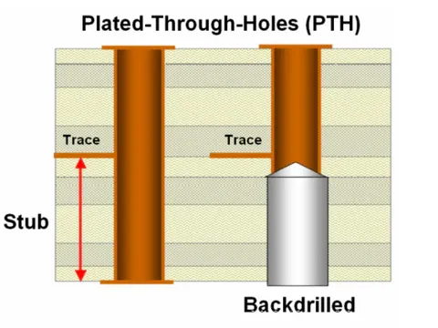
Understanding Via Stubs and Their Impact on High-Speed Signals
A via stub is the unused portion of a through-hole via that extends beyond the layer where a signal transitions. In high-speed designs, these stubs create a problem because they act as resonant structures. For instance, at frequencies above 5 GHz, a stub as short as 0.5 mm can cause significant signal reflections, leading to data errors or signal loss.
The length of the stub determines the resonant frequency at which reflections peak. A longer stub resonates at a lower frequency, while a shorter stub affects higher frequencies. This can result in an impedance mismatch, where the characteristic impedance of the trace (typically 50 ohms for single-ended signals or 100 ohms for differential pairs) is disrupted. The outcome? Increased bit error rates and reduced system reliability.
Controlled depth drilling tackles this issue head-on by physically removing the stub. By drilling from the opposite side of the PCB to a precise depth, only the necessary portion of the via remains conductive, minimizing signal reflections and maintaining impedance control.
The Mechanics of Controlled Depth Drilling in PCB Manufacturing
Controlled depth drilling, often called back drilling, is a precision process that requires advanced machinery and strict manufacturing tolerances. Here’s how it works:
- Design Specification: The PCB designer specifies which vias need back drilling and the exact depth based on the layer stackup. This is often done using design software that outputs detailed drill files.
- Drilling Process: A larger drill bit, typically 0.2 mm wider than the original via hole, is used to remove the conductive material from the stub. The depth is controlled to within 0.1 mm to avoid damaging active layers.
- Inspection: Post-drilling, the board undergoes inspection using techniques like X-ray imaging to ensure accuracy and prevent over-drilling.
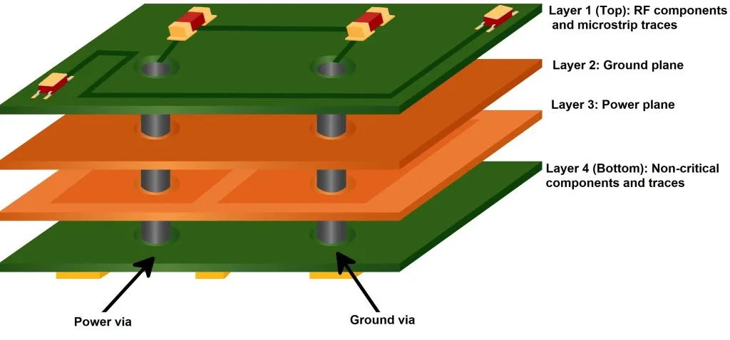
This process is critical for multilayer PCBs with 8 or more layers, where via stubs are more likely to occur due to complex signal routing. By implementing back drilling PCB impedance control, designers can achieve consistent signal performance across all layers.
Benefits of PCB Via Stub Removal for High-Speed Designs
Removing via stubs through controlled depth drilling offers several advantages for high-speed PCB applications. Let’s explore the key benefits:
- Improved Signal Integrity: Eliminating stubs reduces signal reflections, ensuring that high-speed signals maintain their shape and timing. For example, in a 25 Gbps design, back drilling can lower signal loss by up to 30% at critical frequencies.
- Consistent Impedance: Stubs disrupt the characteristic impedance of a trace. By removing them, designers can maintain a stable 50-ohm or 100-ohm impedance, critical for differential signaling in USB 3.0 or PCIe applications.
- Reduced EMI: Via stubs can radiate electromagnetic energy, causing interference. Back drilling minimizes this risk, making it easier to meet strict EMI compliance standards.
- Enhanced Design Flexibility: With stubs removed, engineers have more freedom to route signals through deeper layers without worrying about resonance issues.
These benefits make PCB via stub removal a go-to solution for industries like telecommunications, aerospace, and data centers, where high-speed performance is essential.
High-Speed PCB Design Guidelines for Optimal Results
While controlled depth drilling is a powerful tool, it works best when paired with smart design practices. Here are some high-speed PCB design guidelines to complement back drilling and ensure top-tier signal integrity:
- Minimize Via Usage: Use vias only when necessary. Each via introduces potential stubs and impedance changes. Opt for surface routing or blind vias when possible.
- Optimize Layer Stackup: Design your stackup to keep high-speed signals on outer layers or transition them early to avoid long stubs. A well-planned stackup can reduce the need for extensive back drilling.
- Control Trace Lengths: Match the lengths of differential pairs to within 5 mils (0.127 mm) to prevent skew and timing issues at speeds above 10 Gbps.
- Use Continuous Ground Planes: Place unbroken ground planes beneath high-speed traces to provide a consistent return path, reducing EMI and reflections.
- Simulate Signal Behavior: Use simulation tools to model signal integrity before fabrication. Identify potential stub-related issues and adjust via placement or drilling depth accordingly.
By following these guidelines, you can create designs that maximize the effectiveness of controlled depth drilling and ensure reliable performance in demanding applications.
Minimizing Signal Reflections in PCBs with Precision Drilling
Signal reflections are a major challenge in high-speed designs, often caused by impedance mismatches or unterminated stubs. The key to minimizing signal reflections PCB lies in precision drilling techniques like back drilling. Reflections occur when a signal encounters a change in impedance, sending part of the energy back toward the source. This can distort the signal, leading to errors in data transmission.
Back drilling addresses this by removing the stub, which eliminates the impedance discontinuity at the via. For example, in a 10-layer PCB running at 20 Gbps, a 1 mm stub can cause a reflection coefficient of 0.2, leading to noticeable signal distortion. After back drilling, this coefficient can drop to below 0.05, significantly improving signal clarity.
Additionally, combining back drilling with proper termination techniques (like series or parallel resistors) and controlled impedance traces can further reduce reflections. The result is a cleaner signal path that supports higher data rates with minimal loss.
Challenges and Considerations in Controlled Depth Drilling
While controlled depth drilling offers clear benefits, it’s not without challenges. Understanding these hurdles can help engineers plan better designs and manufacturing processes:
- Cost Implications: Back drilling adds an extra step to PCB fabrication, increasing production costs by 10-20% depending on board complexity. It’s often reserved for high-performance applications where signal integrity justifies the expense.
- Manufacturing Precision: Achieving accurate drill depths requires advanced equipment and skilled operators. A deviation of just 0.05 mm can damage active layers or leave residual stubs.
- Design Complexity: Specifying back drilling for numerous vias in a dense design can complicate the layout and drill files, requiring close collaboration with the manufacturer.
Despite these challenges, the advantages of controlled depth drilling often outweigh the drawbacks, especially for mission-critical systems where performance cannot be compromised.
Applications of Controlled Depth Drilling in Modern Electronics
The demand for high-speed, reliable electronics continues to grow across various industries. Controlled depth drilling plays a pivotal role in enabling these advancements. Here are some key applications:
- Telecommunications: 5G infrastructure relies on PCBs handling frequencies up to 28 GHz. Back drilling ensures signal integrity for base stations and networking equipment.
- Data Centers: Servers and storage systems operating at 56 Gbps or higher use back-drilled PCBs to maintain low latency and high throughput.
- Automotive: Advanced driver-assistance systems (ADAS) require high-speed data processing. Controlled depth drilling supports reliable communication between sensors and control units.
- Aerospace: Avionics systems demand faultless performance under harsh conditions. Back drilling helps meet stringent signal integrity and EMI standards.
These examples highlight why precision drilling techniques are becoming standard in cutting-edge PCB design and manufacturing.
Future Trends in PCB Drilling and Signal Integrity
As electronics continue to push boundaries, PCB manufacturing techniques like controlled depth drilling are evolving. Emerging trends include:
- Automation in Drilling: Advanced CNC machines with real-time depth monitoring are improving precision and reducing human error in back drilling.
- Alternative Via Structures: Blind and buried vias are gaining traction as alternatives to through-hole vias, reducing the need for back drilling in some designs.
- Higher Frequencies: With 6G and beyond on the horizon, signal frequencies may exceed 100 GHz, making precision drilling even more critical for managing reflections and impedance.
Staying ahead of these trends ensures that your PCB designs remain competitive and capable of meeting future demands.
Conclusion: Elevate Your PCB Designs with Precision Drilling
Mastering controlled depth drilling is a game-changer for achieving optimal signal integrity in high-speed PCBs. By addressing via stubs, maintaining impedance control, and minimizing signal reflections, this technique empowers engineers to design boards that perform reliably at data rates of 10 Gbps and beyond. Whether you’re working on telecommunications equipment, data center hardware, or automotive systems, integrating controlled depth drilling PCB signal integrity practices into your workflow can make all the difference.
Pairing precision drilling with thoughtful design strategies, such as optimized stackups and continuous ground planes, further enhances results. While challenges like cost and manufacturing complexity exist, the benefits of cleaner signals and reduced EMI far outweigh the drawbacks for high-performance applications. As technology advances, staying informed about drilling innovations and signal integrity best practices will keep your designs at the forefront of the industry.


