 ALLPCB


In the world of PCB design, ensuring a stable power supply is critical for the performance of electronic devices. Power integrity (PI) and PCB stackups play a vital role in optimizing power distribution networks (PDN). If you're searching for ways to enhance PCB stackup power integrity, improve PDN design, use decoupling capacitors, leverage plane capacitance, and reduce voltage drop, you're in the right place. This blog dives deep into these concepts, offering practical insights and actionable tips to help you design robust and efficient PCBs.
Whether you're an experienced engineer or just starting out, this guide will walk you through the essentials of power integrity and stackup design. Let's explore how to build a PDN that ensures stable voltage, minimizes noise, and supports high-speed circuits.
What is Power Integrity and Why Does It Matter?
Power integrity refers to the ability of a power distribution network to deliver clean, stable power to all components on a PCB. Without proper power integrity, devices can suffer from voltage fluctuations, noise, and signal integrity issues, leading to performance degradation or even failure. In high-speed designs, where components operate at frequencies above 1 GHz, maintaining power integrity becomes even more challenging due to faster switching times and higher current demands.
A well-designed PDN ensures that voltage levels remain within acceptable limits (often within 5% of the nominal value) and minimizes noise that could interfere with sensitive signals. This is where PCB stackups come into play, as they determine how power and ground planes are arranged to support efficient power delivery.
Understanding PCB Stackups for Power Integrity
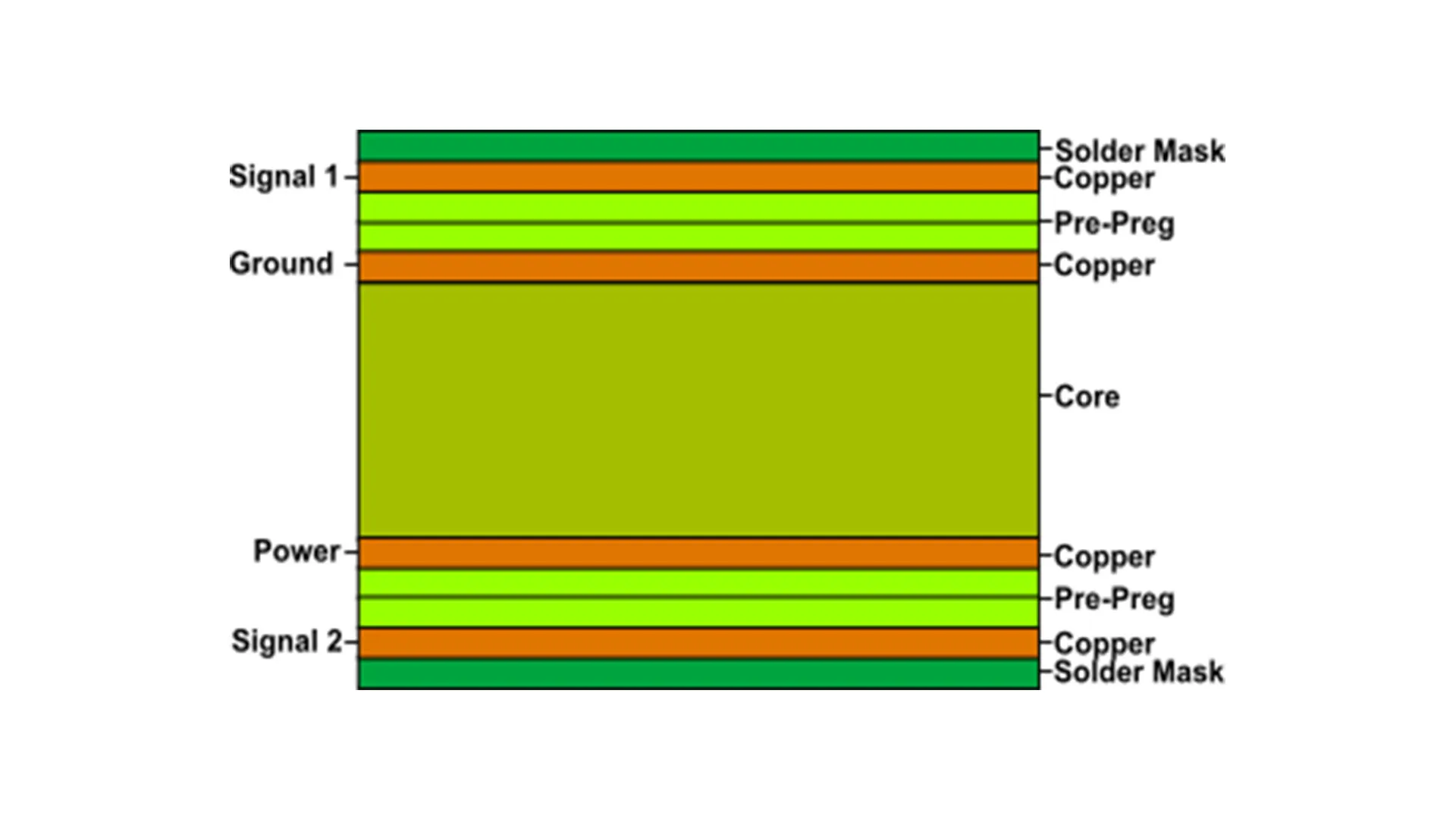
A PCB stackup is the arrangement of conductive and insulating layers in a printed circuit board. A typical stackup might include signal layers, power planes, and ground planes. For power integrity, the placement and configuration of power and ground planes are crucial because they directly impact the impedance of the PDN and the ability to deliver stable power.
In a 4 layer PCB, a common stackup might look like this:
- Top Layer: Signal traces
- Layer 2: Ground plane
- Layer 3: Power plane
- Bottom Layer: Signal traces
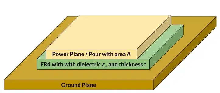
By placing ground and power planes close to each other, you create a natural capacitance (known as plane capacitance) between them. This capacitance helps to stabilize voltage by acting as a small, built-in capacitor, reducing noise and voltage drop. For instance, with a dielectric thickness of 0.1 mm between planes and a dielectric constant of 4.2, the plane capacitance can be calculated as approximately 35 pF per square inch, providing a quick source of charge for nearby components.
In more complex designs, such as 6- or 8-layer boards, additional power and ground planes can be added to support multiple voltage levels and further reduce impedance. The key is to maintain symmetry in the stackup to avoid uneven thermal expansion and ensure balanced electrical performance.
Key Elements of PDN Design for Power Integrity
The power distribution network is the backbone of power integrity. A well-designed PDN minimizes impedance, ensuring that components receive the power they need without significant voltage drops. Let’s break down the critical elements of PDN design.
1. Low Impedance Pathways
Impedance in a PDN is a measure of opposition to current flow. High impedance can lead to voltage drops, especially during sudden current demands (like when a processor switches states). To keep impedance low, use wide power traces or dedicated power planes. For example, a power plane with a thickness of 1 oz copper can handle currents up to 10 A with minimal voltage drop across a 10 cm distance.
2. Proper Use of Decoupling Capacitors
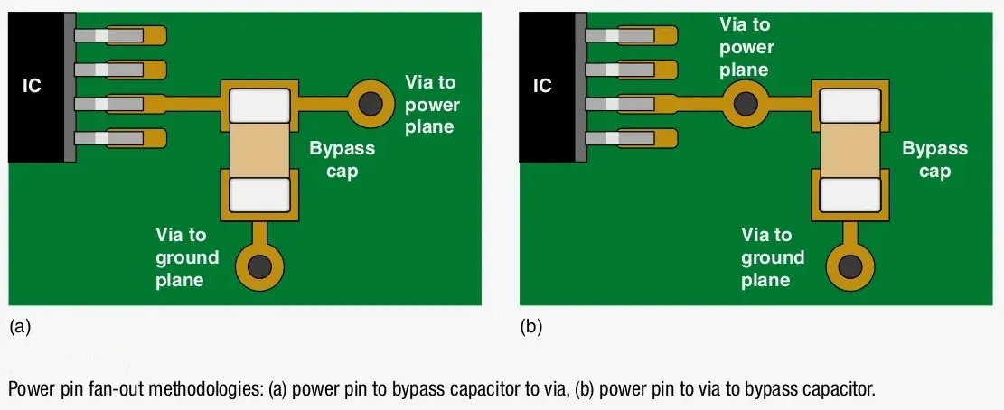
Decoupling capacitors are essential for providing a local source of charge to components, especially during high-frequency switching. They help to smooth out voltage fluctuations and reduce noise. For optimal performance, place decoupling capacitors as close as possible to the power pins of ICs. A common guideline is to use a mix of capacitor values (e.g., 0.1 μF, 1 μF, and 10 μF) to cover a wide range of frequencies, from 100 kHz to 100 MHz.
The placement matters just as much as the value. If a capacitor is placed too far from the IC, parasitic inductance in the traces can reduce its effectiveness. Aim to keep the loop inductance below 1 nH by minimizing the distance and using multiple vias to connect capacitors to power and ground planes.
3. Leveraging Plane Capacitance
As mentioned earlier, plane capacitance is the natural capacitance formed between adjacent power and ground planes. This capacitance acts as a high-frequency filter, helping to stabilize voltage without the need for additional components. To maximize plane capacitance, reduce the dielectric thickness between planes and use materials with a higher dielectric constant. For example, reducing the separation from 0.2 mm to 0.1 mm can double the capacitance per unit area.
4. Reducing Voltage Drop
Voltage drop occurs when current flows through a conductor with resistance, causing a loss of voltage. To minimize reducing voltage drop, use thicker copper layers (e.g., 2 oz instead of 1 oz) for power planes and ensure short, direct connections between the power source and components. Additionally, avoid splitting power planes unnecessarily, as splits can increase impedance and create noise.
For high-current applications, calculate the expected voltage drop using Ohm's Law (V = I * R). If a trace carries 5 A and has a resistance of 0.01 ohms, the voltage drop is 0.05 V, which may be acceptable for a 5 V supply but problematic for a 1.2 V rail.
Best Practices for Optimizing PCB Stackup Power Integrity
Now that we’ve covered the fundamentals, let’s look at actionable strategies to optimize your PCB stackup for power integrity. These tips are designed to help you build a robust PDN that supports both low- and high-speed designs.
1. Prioritize Ground Planes
A solid ground plane is the foundation of a good PDN. It provides a low-impedance return path for currents and helps to shield sensitive signals from noise. Avoid cutting or splitting ground planes unless absolutely necessary, as this can create impedance discontinuities and increase electromagnetic interference (EMI).
2. Use Multiple Power Planes for Complex Designs
In designs with multiple voltage levels (e.g., 3.3 V, 1.8 V, and 1.2 V), dedicate separate power planes or sections to each voltage. This prevents cross-talk between different power domains and ensures that each component receives clean power. Use ferrite beads or inductors to isolate power domains if needed.
3. Optimize Via Placement
Vias connect layers in a PCB, but they introduce inductance and resistance. For power delivery, use multiple vias in parallel to reduce inductance when connecting decoupling capacitors or power pins to planes. A single via might have an inductance of 0.5 nH, but using four vias in parallel can lower it to 0.125 nH.
4. Simulate Your PDN
Simulation tools can help you analyze the impedance profile of your PDN and identify potential issues before manufacturing. These tools model the behavior of power planes, capacitors, and traces to predict voltage drops and noise levels. Aim for a target impedance below 1 ohm across the operating frequency range of your design (e.g., DC to 100 MHz) to ensure stable power delivery.
Common Challenges in PDN Design and How to Overcome Them
Designing a PDN for optimal power integrity isn’t without challenges. Here are some common issues and solutions to help you navigate them.
1. Resonances in the PDN
At certain frequencies, the interaction between capacitors and plane capacitance can create resonances, leading to high impedance peaks. To mitigate this, use capacitors with higher equivalent series resistance (ESR) in specific cases, as ESR can dampen resonances. Alternatively, spread out capacitor values to cover a broader frequency range.
2. High-Frequency Noise
High-frequency noise often comes from fast-switching components like processors or FPGAs. Place high-frequency decoupling capacitors (e.g., 0.1 μF) as close as possible to the noise source, and ensure that power and ground planes are tightly coupled to maximize plane capacitance.
3. Limited Board Space
In compact designs, there may not be enough room for all the decoupling capacitors or wide power planes. In such cases, prioritize capacitors for the most critical components and use embedded capacitance materials to increase plane capacitance without adding extra layers.
Conclusion: Building Better PCBs with Power Integrity
Power integrity and PCB stackups are inseparable when it comes to designing reliable electronic systems. By focusing on PCB stackup power integrity, refining your PDN design, strategically placing decoupling capacitors, utilizing plane capacitance, and actively working on reducing voltage drop, you can create a power distribution network that supports high performance and minimizes noise.
Start by designing a balanced stackup with closely coupled power and ground planes. Add decoupling capacitors where they’re needed most, and use simulation tools to validate your design. With these practices, you’ll be well on your way to building PCBs that deliver stable, clean power to every component.
At ALLPCB, we’re committed to supporting engineers with resources and manufacturing solutions to bring their designs to life. Apply these principles in your next project, and watch your designs perform at their best.


