 ALLPCB


Are you looking to reduce costs and improve efficiency in your PCB projects? Understanding the relationship between PCB size and cost is key to achieving both. In this comprehensive guide, we’ll explore how to optimize your board design for maximum efficiency through smart sizing, material selection, and manufacturing strategies. By focusing on PCB size and cost analysis, PCB cost optimization, PCB material costs, PCB manufacturing costs, and PCB design for cost reduction, you’ll learn actionable tips to save money without compromising quality. Let’s dive into the details!
Why PCB Size and Cost Matter in Design
When designing a printed circuit board (PCB), size and cost are two of the most critical factors to consider. A larger board often means higher material and manufacturing expenses, while a smaller board can save money but may limit functionality or complicate assembly. Striking the right balance is essential for efficiency. By conducting a thorough PCB size and cost analysis, you can identify opportunities to minimize expenses while ensuring your design meets performance requirements.
In the sections below, we’ll break down the factors that influence PCB costs, including size, materials, and manufacturing processes. We’ll also share proven strategies for PCB cost optimization to help you make informed decisions at every stage of your project.
Key Factors Influencing PCB Costs
Before diving into optimization techniques, it’s important to understand the main elements that drive PCB costs. These include board size, material selection, layer count, and manufacturing processes. Let’s explore each of these in detail.
1. PCB Size and Its Impact on Cost
The physical dimensions of your PCB directly affect the cost. Larger boards require more raw materials, such as substrate and copper, which increase PCB material costs. Additionally, bigger boards take up more space on manufacturing panels, reducing the number of boards that can be produced in a single run. This inefficiency often leads to higher PCB manufacturing costs.
For example, a standard panel size in PCB production is often 18 x 24 inches. If your board measures 6 x 6 inches, only a few units can fit on a panel, driving up the cost per board. However, reducing the size to 3 x 3 inches could allow more boards per panel, significantly lowering the cost per unit.
2. Material Selection and Costs
The materials used in your PCB also play a big role in determining cost. Standard materials like FR-4 are widely used and affordable, often costing between $0.50 to $1.00 per square inch for basic designs. However, if your project requires high-frequency performance or thermal resistance, you might need specialized materials like Rogers or polyimide, which can cost 2-5 times more per square inch.
Balancing performance needs with PCB material costs is crucial. Choosing a cost-effective material that still meets your design requirements can lead to significant savings.
3. Layer Count and Complexity
The number of layers in your PCB directly correlates with cost. A single-layer board is the cheapest to produce, while a 4-layer or 6-layer board can cost 2-3 times more due to additional materials and manufacturing steps. Each layer adds complexity to the design and increases the risk of errors, further driving up PCB manufacturing costs.
For instance, a 2-layer board might cost $0.10 per square inch to fabricate, while a 6-layer board could jump to $0.30 per square inch or more, depending on the design complexity.
4. Manufacturing Processes and Lead Times
The manufacturing process itself impacts cost. Processes like surface finish (e.g., HASL vs. ENIG) and via types (e.g., through-hole vs. microvias) can add to expenses. Additionally, shorter lead times often come with a premium price, as manufacturers prioritize your order over others.
By planning ahead and allowing for standard lead times, you can avoid rush fees and reduce PCB manufacturing costs. Standard lead times are typically 5-10 days for basic boards, while expedited orders (2-3 days) can increase costs by 20-50%.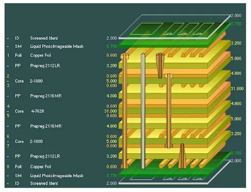
Strategies for PCB Cost Optimization
Now that we’ve covered the factors driving PCB costs, let’s look at practical strategies for PCB cost optimization. These tips will help you design boards that are both cost-effective and efficient.
1. Optimize PCB Size for Panelization
One of the most effective ways to reduce costs is to design your PCB size with panelization in mind. Panelization refers to arranging multiple PCBs on a single manufacturing panel to maximize the use of space. By fitting more boards onto a panel, you lower the cost per unit.
For example, if a panel can hold 10 boards of 4 x 4 inches but only 5 boards of 6 x 6 inches, the smaller design will be more cost-efficient. Work with your manufacturer to understand their standard panel sizes and design your board dimensions accordingly. This simple step can cut PCB manufacturing costs by 10-20% or more.
2. Minimize Layer Count
Reducing the number of layers in your PCB is another powerful way to save money. If your design can function with a 2-layer board instead of a 4-layer one, you could halve your fabrication costs. Carefully analyze your circuit requirements and routing needs to determine the minimum number of layers necessary.
For instance, if your design involves low-speed signals (below 50 MHz), a 2-layer board is often sufficient. However, high-speed designs (above 100 MHz) may require additional layers for impedance control and signal integrity.
3. Choose Cost-Effective Materials
As mentioned earlier, material selection is a major factor in PCB material costs. Stick to standard materials like FR-4 for general-purpose applications. Reserve high-cost materials for projects where specific properties, such as high thermal conductivity or low dielectric loss, are essential.
Additionally, consider using thinner substrates if your design allows. A 1.6mm thick FR-4 board is standard and cost-effective, but a 0.8mm board can reduce material usage and weight, saving a small percentage on costs.
4. Simplify Design for Manufacturability
Designing your PCB with manufacturability in mind can significantly lower costs. Avoid overly complex features like very small vias (below 0.3mm) or tight trace spacing (below 6 mils), as these require advanced manufacturing techniques that increase expenses.
For example, using standard drill sizes for vias (0.4mm or larger) and maintaining a trace width of 8 mils or more can keep your design within standard manufacturing capabilities, reducing PCB manufacturing costs by avoiding special processes.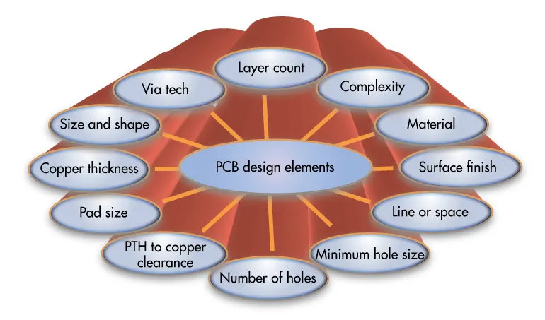
PCB Design for Cost Reduction: Advanced Techniques
Beyond the basics, there are advanced techniques in PCB design for cost reduction that can further optimize your project. These strategies require a deeper understanding of design and manufacturing but can yield substantial savings.
1. Use Standard Components and Footprints
Choosing standard components with widely available footprints reduces assembly costs. Custom or rare components often require special handling or sourcing, which drives up expenses. Stick to components with common packages like 0805 or 0603 for resistors and capacitors, as these are cost-effective and easy to source.
For example, using a standard 0805 resistor footprint instead of a custom size can save on both component and assembly costs, as automated pick-and-place machines are optimized for standard sizes.
2. Optimize Routing for Signal Integrity
Efficient routing not only improves performance but also reduces costs by minimizing the need for additional layers. For high-speed signals, maintain controlled impedance by using consistent trace widths and spacing. A common target for impedance is 50 ohms for single-ended signals, which can often be achieved on a 2-layer board with proper design.
By optimizing routing, you can avoid the need for extra layers, saving on PCB manufacturing costs while ensuring signal integrity.
3. Leverage Design Software for Cost Analysis
Modern design software often includes tools for cost estimation and design rule checking. Use these features to simulate manufacturing costs based on your board size, layer count, and material choices. This allows you to make adjustments early in the design process, avoiding costly revisions later.
For instance, some tools can estimate the cost difference between a 2-layer and 4-layer design, helping you make data-driven decisions for PCB cost optimization.
Balancing Cost and Performance: Practical Tips
While cost reduction is important, it should never come at the expense of performance or reliability. Here are some practical tips to balance cost and quality in your PCB projects.
1. Prioritize Critical Design Requirements
Identify the non-negotiable aspects of your design, such as signal speed or thermal management, and allocate your budget accordingly. For example, if your application involves high-speed data transfer at 500 MHz, investing in a 4-layer board with controlled impedance traces is worth the added cost to avoid signal degradation.
2. Test Prototypes Before Full Production
Prototyping is a cost-effective way to identify design flaws before committing to a full production run. A single prototype might cost $50-$100, but it can save thousands by preventing errors in a batch of 1,000 boards. Use prototypes to validate your design choices and ensure they meet both cost and performance goals.
3. Collaborate with Manufacturers Early
Engaging with your manufacturing partner during the design phase can uncover cost-saving opportunities. Manufacturers can provide insights on panelization, material availability, and standard processes that align with your PCB size and cost analysis. This collaboration often leads to better pricing and fewer production delays.
Conclusion: Achieving Efficiency Through Smart PCB Design
Optimizing your PCB for maximum efficiency involves a careful balance of size, materials, and design choices. By conducting a thorough PCB size and cost analysis, focusing on PCB cost optimization, and applying strategies for PCB design for cost reduction, you can significantly lower PCB material costs and PCB manufacturing costs without sacrificing quality.
Start by designing with panelization in mind, choosing cost-effective materials, and minimizing layer count. Then, apply advanced techniques like standard component selection and efficient routing to further reduce expenses. Finally, prioritize critical requirements and test prototypes to ensure your design performs as expected.
With these strategies, you’ll be well-equipped to create cost-effective, high-performing PCBs for any project. Take control of your design process today and see the savings add up!


