 ALLPCB


In high-speed PCB design, optimizing trace width is critical for maintaining signal integrity. The width of a trace directly impacts impedance, reduces signal reflection, and ensures reliable performance in your circuits. But how do you determine the right trace width for your design? This guide offers a clear, practical approach to balancing trace width with signal integrity, focusing on impedance control and minimizing reflections. Let’s dive into the details of achieving optimal performance for your high-speed PCB layouts.
Why Trace Width Matters for Signal Integrity
Signal integrity refers to the quality of an electrical signal as it travels through a PCB. In high-speed designs, where signals switch at frequencies above 100 MHz, even small issues like impedance mismatches or reflections can cause data errors, crosstalk, or electromagnetic interference (EMI). Trace width plays a major role in controlling these factors.
A trace that’s too narrow may increase resistance and lead to voltage drops or overheating. On the other hand, a trace that’s too wide can cause impedance mismatches, resulting in signal reflections that distort the waveform. Finding the right trace width ensures that signals travel with minimal loss and distortion, which is essential for applications like USB, HDMI, or DDR memory interfaces.

Understanding Impedance and Its Relation to Trace Width
Impedance, measured in ohms, is the opposition a trace offers to the flow of alternating current (AC) signals. In high-speed PCB design, maintaining a consistent impedance—often 50 ohms or 75 ohms depending on the application—is vital for signal integrity. Trace width is a key factor in controlling this impedance.
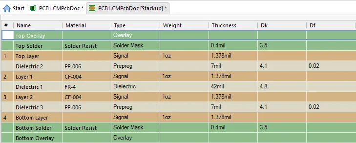
The impedance of a trace depends on several elements: the width of the trace, the thickness of the copper, the dielectric constant of the PCB material (often denoted as Dk), and the distance to the ground plane. A wider trace generally lowers impedance, while a narrower trace increases it. For instance, in a microstrip configuration (a trace on the outer layer of a PCB with a ground plane beneath), a trace width of 6 mils on a standard FR-4 material with a dielectric constant of 4.2 might achieve a 50-ohm impedance if the ground plane is 8 mils away. Adjust any of these values, and the impedance changes.
To calculate the correct trace width for a specific impedance, designers often use online calculators or simulation software. These tools take into account the PCB stack-up and material properties to provide precise width recommendations. Without proper impedance control, signals can reflect back along the trace, causing interference and degrading performance.
Signal Reflection: How Trace Width Impacts Waveforms
Signal reflection occurs when a signal encounters a sudden change in impedance along its path, sending part of the signal back toward the source. This can happen if the trace width varies or if there’s a mismatch between the trace impedance and the load or source impedance. Reflections distort the signal, leading to issues like ringing, overshoot, or data loss in high-speed PCB designs.
Optimizing trace width helps minimize these reflections by maintaining consistent impedance. For example, in a high-speed design operating at 1 GHz, even a small mismatch—say, a trace impedance of 55 ohms instead of the target 50 ohms—can cause significant reflections. Keeping trace width uniform and matching it to the required impedance ensures the signal travels smoothly without bouncing back.
Another practical tip is to avoid abrupt changes in trace geometry. If a trace must widen or narrow due to space constraints, use a gradual taper rather than a sharp transition to reduce impedance discontinuities. This small adjustment can make a big difference in reducing signal reflection.
Key Factors in Optimizing Trace Width for High-Speed PCB Design
When designing a PCB for high-speed signals, several factors beyond just trace width come into play. Let’s break down the most important considerations to ensure signal integrity.
1. PCB Material and Dielectric Constant
The material of your PCB affects how signals propagate. Most standard PCBs use FR-4, which has a dielectric constant (Dk) of about 4.2 to 4.5 at 1 MHz. However, at higher frequencies, this value can vary, impacting impedance. If your design operates above 5 GHz, consider using low-loss materials with a more stable Dk, such as Rogers or Isola laminates. The dielectric constant influences the trace width needed for a specific impedance, so always check the material specs before finalizing your design.
2. Copper Thickness
Copper thickness, typically measured in ounces per square foot (oz/ft2), also affects trace impedance. Common thicknesses are 1 oz (35 μm) and 2 oz (70 μm). Thicker copper lowers resistance, which is good for power delivery, but it can slightly alter impedance in high-speed signal traces. When calculating trace width, factor in the copper thickness to ensure accurate impedance matching.
3. Trace Spacing and Ground Planes
In high-speed designs, traces should be spaced adequately to avoid crosstalk, where signals on adjacent traces interfere with each other. A general rule is to keep trace spacing at least three times the trace width (3W rule) for minimal coupling. Additionally, a solid ground plane beneath signal traces provides a return path for currents, stabilizing impedance and reducing EMI. The distance between the trace and ground plane also impacts impedance, so maintain a consistent separation throughout the design.
4. Frequency of Operation
The frequency of your signals determines how critical trace width optimization becomes. At low frequencies (below 100 MHz), small variations in trace width may not significantly affect performance. However, at higher frequencies (1 GHz and above), even a 1-mil deviation in width can cause noticeable impedance changes. For example, a USB 3.0 design running at 5 Gbps requires precise trace widths to maintain a 90-ohm differential impedance, while older USB 2.0 at 480 Mbps is more forgiving.
Practical Steps to Optimize Trace Width
Now that we’ve covered the theory, let’s walk through actionable steps to optimize trace width for signal integrity in your high-speed PCB designs.
Step 1: Define Impedance Requirements
Start by identifying the target impedance for your signals. Common standards include 50 ohms for single-ended signals (like RF or coaxial connections) and 100 ohms for differential pairs (like Ethernet or USB). Check the specifications of the components or protocols you’re working with to confirm the required impedance.
Step 2: Use a Trace Width Calculator
Manually calculating trace width can be complex due to the many variables involved. Instead, use a reliable trace width calculator or simulation tool. Input parameters like target impedance, dielectric constant, copper thickness, and ground plane spacing to get the recommended trace width. For instance, a 50-ohm trace on a 1.6 mm FR-4 board with a 1 oz copper layer might require a width of around 11 mils, but this varies with stack-up.
Step 3: Simulate and Validate
After determining the trace width, simulate your design using software tools to check for impedance mismatches or signal reflections. Look for issues like overshoot or ringing in the simulated waveforms. If discrepancies arise, adjust the trace width or other parameters and re-simulate until the results align with your requirements.
Step 4: Maintain Consistency in Layout
During PCB layout, ensure that trace widths remain uniform along the signal path. Avoid unnecessary bends or changes in width, as these can cause impedance discontinuities. If a trace must cross layers, use vias carefully and match the impedance as closely as possible. Route high-speed traces over a continuous ground plane to provide a stable return path.

Common Mistakes to Avoid in Trace Width Optimization
Even experienced designers can make errors when optimizing trace width. Here are some pitfalls to watch out for in high-speed PCB design:
- Ignoring Stack-Up Design: Failing to account for the PCB layer stack-up can lead to incorrect impedance calculations. Always consider the full stack-up, including dielectric layers and ground planes, when determining trace width.
- Neglecting Temperature Effects: High-speed signals can generate heat, and trace resistance increases with temperature. Ensure your trace width can handle the current without excessive heating, which could alter impedance.
- Overlooking Manufacturing Tolerances: PCB fabrication processes have tolerances, typically ±10% for trace width. Design with these variations in mind to ensure the final product maintains signal integrity.
Advanced Tips for High-Speed PCB Design
For cutting-edge designs operating at frequencies above 10 GHz, additional strategies can further enhance signal integrity:
- Differential Pair Routing: In differential signaling, match the lengths and widths of paired traces to maintain consistent impedance and minimize skew. A common target is 100 ohms for differential pairs, often requiring precise width adjustments.
- Low-Loss Materials: At very high frequencies, standard FR-4 may introduce significant signal loss. Switching to advanced laminates with lower dielectric loss can preserve signal quality, though it impacts trace width calculations.
- Back-Drilling Vias: For multilayer boards, unused via stubs can cause reflections. Back-drilling removes these stubs, improving signal integrity without altering trace width.
Conclusion: Achieving Signal Integrity Through Trace Width Optimization
Optimizing trace width is a fundamental step in ensuring signal integrity for high-speed PCB designs. By carefully calculating trace width to match the desired impedance, minimizing signal reflections, and considering factors like PCB material and frequency, you can create reliable and efficient circuits. Follow the practical steps outlined in this guide—defining impedance, using calculators, simulating designs, and maintaining layout consistency—to achieve optimal performance.
Whether you’re designing for USB, Ethernet, or RF applications, paying attention to trace width and its impact on impedance will elevate the quality of your PCBs. With the right approach, you can tackle the challenges of high-speed design and deliver products that meet the demands of modern electronics.


