 ALLPCB


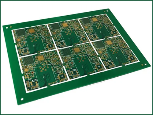
Are you looking to understand the multi-layer PCB manufacturing process? Multi-layer PCBs are essential for complex electronics, offering compact designs and high performance. In this comprehensive guide, we’ll walk you through every step of multi-layer PCB fabrication steps, from design to testing, including multi-layer PCB assembly, multi-layer PCB testing, and multi-layer PCB quality control. Whether you're an engineer or a hobbyist, this deep dive will help you grasp the intricate production process behind these advanced circuit boards.
What Are Multi-Layer PCBs and Why Are They Important?
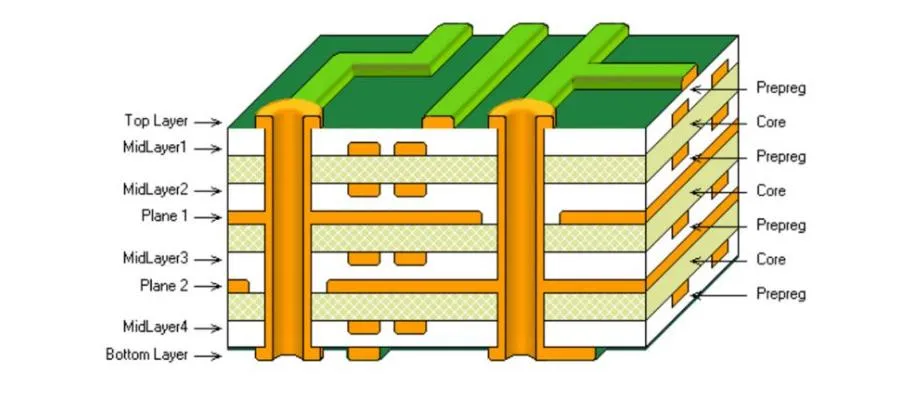
Multi-layer PCBs are printed circuit boards with more than two layers of conductive copper, separated by insulating materials. Unlike single or double-layer boards, they can have 4, 6, 8, or even up to 48 layers, depending on the complexity of the design. These boards are crucial for modern electronics like smartphones, medical devices, and automotive systems because they allow for higher component density and better signal integrity.
The compact design of multi-layer PCBs reduces the size of devices while supporting high-speed signals—often exceeding 10 GHz in advanced applications. They also improve electromagnetic compatibility (EMC) by minimizing interference through dedicated ground and power planes. Understanding the multi-layer PCB manufacturing process is key to leveraging their benefits in your projects.
Overview of the Multi-Layer PCB Manufacturing Process
The multi-layer PCB manufacturing process involves multiple stages, each requiring precision to ensure the final product meets strict performance and reliability standards. Below, we break down the multi-layer PCB fabrication steps into detailed sections to give you a clear picture of how these boards are made.
1. Design and Pre-Production Preparation
The journey begins with the design phase. Engineers use specialized software to create a schematic and layout for the multi-layer PCB. This step defines the placement of components, routing of traces, and layer stack-up. For high-speed designs, impedance control is critical, often targeting values like 50 ohms for signal integrity.
Once the design is finalized, it undergoes a Design for Manufacturability (DFM) check to ensure it meets production tolerances—such as minimum trace widths of 0.1 mm and via sizes of 0.2 mm. The design files are then converted into Gerber files, which act as blueprints for manufacturing. This pre-production step is vital to avoid costly errors during fabrication.
2. Material Selection and Preparation
Multi-layer PCBs are typically made using FR-4, a fiberglass-reinforced epoxy laminate, as the base material. For high-frequency applications, materials like Rogers or Teflon may be used due to their low dielectric constant (often around 2.2 to 3.5) and minimal signal loss. Copper foil, usually 1 oz (35 microns thick), is laminated onto the substrate to form conductive layers.
The materials are cut into panels, cleaned, and prepared for the next steps. Proper material selection ensures the board can withstand thermal stress and maintain performance under operating conditions.
3. Inner Layer Processing
The inner layers of a multi-layer PCB are processed first. A photoresist layer is applied to the copper-clad panels, and the design pattern is transferred using UV light exposure. Unwanted copper is etched away, leaving behind the circuit traces. For a 4-layer board, this step might create two inner layers with traces as narrow as 0.15 mm for dense designs.
After etching, the layers undergo Automated Optical Inspection (AOI) to detect defects like open circuits or shorts. This early quality check is a cornerstone of multi-layer PCB quality control, ensuring issues are caught before lamination.
4. Lamination of Layers
Once the inner layers are ready, they are stacked with prepreg (pre-impregnated resin sheets) as insulators between them. The stack is then pressed under high temperature (around 180°C) and pressure (up to 500 psi) to bond the layers into a single panel. This process must be precise to avoid misalignment, which could disrupt signal paths or via connections.
The laminated panel forms the core structure of the multi-layer PCB, ready for drilling and further processing. This step is critical in the multi-layer PCB fabrication steps as it determines the board’s structural integrity.
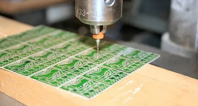
5. Drilling and Via Formation
Next, holes are drilled into the panel for vias and component mounting. Vias are tiny holes (often 0.2 to 0.5 mm in diameter) that connect different layers electrically. In multi-layer PCBs, blind and buried vias are common, requiring precise drilling techniques like laser drilling for accuracy within 0.05 mm.
After drilling, the holes are cleaned to remove debris, ensuring smooth copper plating in the next step. This process is essential for maintaining connectivity across layers in complex designs.
6. Copper Plating and Outer Layer Processing
The drilled panel undergoes electroless copper plating to create a thin conductive layer inside the vias. Then, electroplating adds a thicker copper layer (typically 25-35 microns) to strengthen the connections. The outer layers are patterned and etched similarly to the inner layers, forming the final circuit design.
This step ensures robust electrical connections and prepares the board for surface finishing, a key part of the multi-layer PCB manufacturing process.
7. Surface Finishing
Surface finishing protects the exposed copper from oxidation and enhances solderability. Common finishes include HASL (Hot Air Solder Leveling), ENIG (Electroless Nickel Immersion Gold), and OSP (Organic Solderability Preservative). For high-reliability applications, ENIG is preferred due to its flat surface and corrosion resistance, with a gold layer thickness of about 0.05 to 0.1 microns.
The choice of finish impacts the board’s performance during multi-layer PCB assembly and long-term durability.
8. Solder Mask and Silkscreen Application
A solder mask, usually green, is applied to protect the copper traces and prevent short circuits during soldering. It covers all areas except pads and vias where components will be mounted. The silkscreen layer adds labels, logos, and component identifiers using white ink for easy assembly reference.
These finishing touches are crucial for both functionality and user-friendliness in the final product.
Multi-Layer PCB Assembly: Bringing the Board to Life
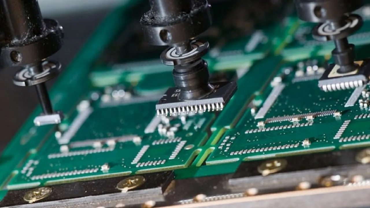
After fabrication, the next stage is multi-layer PCB assembly. This process involves placing and soldering components onto the board. Here’s how it works:
- Solder Paste Application: Solder paste is printed onto the pads using a stencil. This paste, a mix of tiny solder particles and flux, temporarily holds components in place.
- Component Placement: Surface Mount Technology (SMT) machines place components with precision, often handling thousands of parts per hour. For fine-pitch components, placement accuracy is within 0.01 mm.
- Reflow Soldering: The board passes through a reflow oven, heating the solder paste to around 250°C to create permanent connections.
- Through-Hole Assembly (if applicable): For components with leads, manual or wave soldering is used to secure them.
Assembly requires meticulous attention to detail to avoid issues like tombstoning or cold solder joints, which can compromise performance.
Multi-Layer PCB Testing: Ensuring Reliability
Testing is a critical part of the multi-layer PCB manufacturing process. Multi-layer PCB testing verifies that the board functions as intended and meets design specifications. Common testing methods include:
- In-Circuit Testing (ICT): Checks for shorts, opens, and component values using a bed-of-nails fixture.
- Functional Testing: Simulates real-world operation to ensure the board performs its intended tasks.
- Flying Probe Testing: Uses movable probes to test electrical connectivity, ideal for prototypes or small batches.
- Automated Optical Inspection (AOI): Detects visual defects like misaligned components or solder issues.
For high-speed boards, signal integrity tests measure parameters like crosstalk and impedance, ensuring values stay within tolerances (e.g., ±10% of 50 ohms). Testing is a non-negotiable step in multi-layer PCB quality control.
Multi-Layer PCB Quality Control: Standards and Best Practices
Multi-layer PCB quality control ensures the final product is reliable and defect-free. Manufacturers adhere to industry standards like IPC-6012 for performance and reliability. Key quality control practices include:
- Material Inspection: Verifying raw materials meet dielectric and thermal specifications.
- Process Monitoring: Continuous checks during lamination, drilling, and plating to maintain tolerances.
- Final Inspection: Visual and electrical tests before shipping to confirm compliance with customer requirements.
Quality control at every stage prevents costly rework and ensures the boards can handle demanding applications without failure.
Challenges in Multi-Layer PCB Manufacturing
Producing multi-layer PCBs comes with unique challenges. Misalignment during lamination can cause signal issues, while improper drilling may lead to broken vias. High-layer-count boards (e.g., 12+ layers) require tighter control over thermal expansion, as even a 0.1% mismatch can warp the board.
Additionally, maintaining signal integrity in high-speed designs demands precise impedance matching and minimal crosstalk. Manufacturers must balance cost, complexity, and performance to deliver reliable boards.
Why Choose Professional Services for Multi-Layer PCB Manufacturing?
Partnering with experienced manufacturers ensures access to advanced equipment, skilled technicians, and rigorous quality control. Professional services streamline the multi-layer PCB manufacturing process, from design optimization to final testing, saving time and reducing errors. They also offer expertise in handling complex designs with tight tolerances, ensuring your project meets industry standards.
Conclusion: Mastering Multi-Layer PCB Production
The multi-layer PCB manufacturing process is a complex but fascinating journey, encompassing detailed multi-layer PCB fabrication steps, precise multi-layer PCB assembly, thorough multi-layer PCB testing, and strict multi-layer PCB quality control. Each stage, from design to final inspection, plays a vital role in creating high-performance boards for today’s advanced electronics.
By understanding these processes, you can make informed decisions for your projects, ensuring optimal results. Whether you’re designing compact consumer gadgets or critical industrial systems, multi-layer PCBs are the backbone of innovation, and mastering their production is key to success.


