ALLPCB


Are you looking to speed up your prototyping process by etching multiple PCBs at once? Multi-board panelization is the answer. This technique allows you to design, etch, and fabricate several printed circuit boards (PCBs) on a single panel, saving time and resources, especially for home PCB fabrication and DIY etching projects. In this comprehensive guide, we'll walk you through the process of PCB etching panelization, share practical tips for etching multiple boards, and provide step-by-step instructions tailored for faster prototyping.
What Is Multi-Board Panelization and Why Does It Matter?
Multi-board panelization is the process of arranging multiple PCB designs on a single larger panel for fabrication or etching. Instead of handling each board individually, you create a single layout that contains several smaller boards, which can be etched, drilled, and separated later. This method is a game-changer for both hobbyists and professionals engaged in DIY etching techniques or small-batch prototyping.
The benefits are clear: it reduces material waste, cuts down on processing time, and ensures consistency across boards since they’re all etched under the same conditions. For home PCB fabrication, panelization can make the process more efficient by minimizing the number of times you need to handle chemicals or repeat steps. Whether you're working on a small project or testing multiple iterations of a design, this approach can save hours of effort.
Advantages of Etching Multiple Boards with Panelization
Before diving into the how-to, let’s explore why PCB etching panelization is worth considering:
- Time Efficiency: Etching multiple boards at once means fewer cycles of preparing, exposing, and cleaning. For instance, if each board takes 30 minutes to etch individually, panelizing four boards could reduce your total etching time to just over 30 minutes instead of 2 hours.
- Cost Savings: By using one large panel, you optimize the use of copper-clad boards and chemicals, reducing waste in home PCB fabrication.
- Consistency: Since all boards on the panel are processed together, they experience the same exposure times and chemical concentrations, leading to uniform results.
- Scalability: Panelization is ideal for prototyping multiple designs or producing small batches, making it a versatile technique for DIY enthusiasts.
Step-by-Step Guide to Panelization for PCB Etching
Now that you understand the benefits, let’s break down the process of panelizing and etching multiple boards. This guide focuses on home PCB fabrication, using accessible tools and DIY etching techniques.
Step 1: Design Your Individual PCBs
Start by creating the designs for each individual PCB using your preferred design software. Ensure that each layout is finalized, with all traces, pads, and components placed correctly. Double-check for errors, as mistakes at this stage will replicate across the panel. For best results, keep the dimensions of each board consistent if possible, as this simplifies panel arrangement.
Pay attention to trace widths and spacing. For example, a common trace width for prototyping is 0.010 inches (10 mils), with a minimum spacing of 0.008 inches (8 mils) to avoid short circuits during etching.
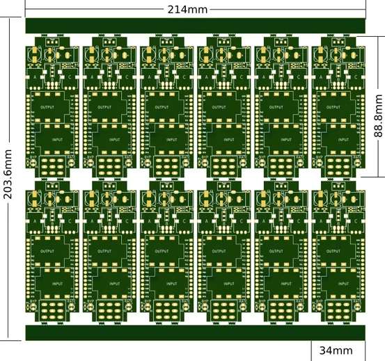
Step 2: Arrange Multiple Boards into a Panel
Once your individual designs are ready, combine them into a single panel layout. Most design tools allow you to import multiple board files and arrange them manually. Leave a small gap, typically 0.1 to 0.2 inches (2.5 to 5 mm), between each board to allow for separation after etching. You can also add breakaway tabs or scoring lines to make it easier to snap the boards apart later.
For home PCB fabrication, ensure the panel size fits within the dimensions of your copper-clad board and etching tank. A typical panel size for hobbyists might be 6 x 6 inches (15 x 15 cm), accommodating four 2 x 2 inch (5 x 5 cm) boards.
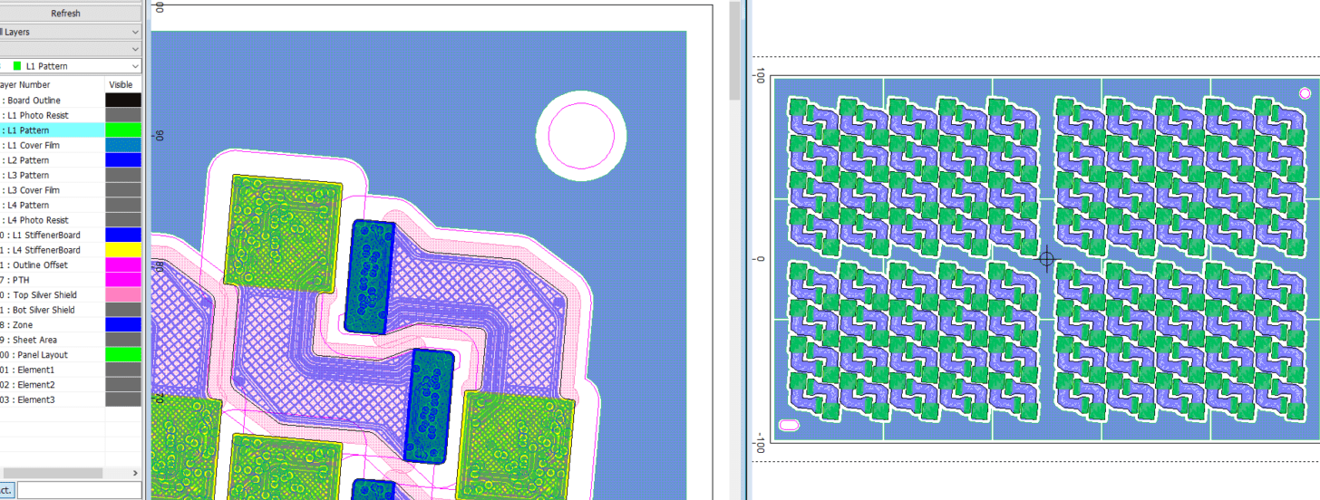
Step 3: Add Panel Features
To make fabrication easier, add features like fiducial marks (small reference points for alignment) and tooling holes (for securing the panel during drilling). If you’re planning to separate the boards manually, include V-grooves or mouse bites—small perforated holes along the edges of each board. Mouse bites typically consist of 5 to 10 small holes, each 0.02 inches (0.5 mm) in diameter, spaced closely together.
These features ensure precision during etching and help avoid damaging individual boards when separating them from the panel.
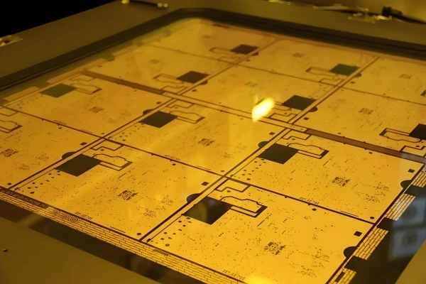
Step 4: Prepare the Panel for Etching
Print your panel design onto a transparency or transfer paper, depending on your etching method. For home PCB fabrication, the toner transfer method is popular and cost-effective. Heat-transfer the design onto a copper-clad board using an iron or laminator, ensuring the toner adheres evenly across the entire panel.
If you’re using photoresist, expose the panel under UV light through the transparency for about 5 to 10 minutes, depending on your setup. Develop the photoresist in a developer solution to reveal the copper areas to be etched.
Step 5: Etch the Panel
Place the prepared panel into an etching solution, such as ferric chloride or a mix of hydrogen peroxide and hydrochloric acid. For a panel of 6 x 6 inches, etching might take 20 to 40 minutes at room temperature (around 25°C or 77°F), depending on the solution’s strength and copper thickness (typically 1 oz or 35 μm for standard boards).
Agitate the solution gently to ensure even etching across all boards on the panel. Check periodically to avoid over-etching, which can damage fine traces. Once the unwanted copper is removed, rinse the panel with water to stop the etching process.
Step 6: Clean and Separate the Boards
After etching, clean the panel with acetone or alcohol to remove any remaining toner or photoresist. Inspect each board for defects like incomplete traces or over-etched areas. If everything looks good, use a saw, rotary tool, or simply snap the boards apart along the breakaway tabs or mouse bites.
For V-grooves, a light scoring with a utility knife along the lines can help with clean separation. Be cautious to avoid stressing the boards, as this can cause cracks or delamination.
Tips for Successful PCB Etching Panelization at Home
Etching multiple boards using panelization can be straightforward, but small mistakes can lead to wasted materials. Here are some practical tips to ensure success with DIY etching techniques:
- Use Consistent Board Sizes: If possible, design boards with identical dimensions to simplify panel layout and separation. For example, four 2 x 3 inch boards fit neatly on a 6 x 6 inch panel with minimal wasted space.
- Protect Edges During Etching: Apply a layer of tape or resist along the panel edges to prevent over-etching at the borders, which can weaken the copper near cut lines.
- Monitor Etching Time: Over-etching can reduce trace widths below safe levels. For a 10-mil trace, over-etching by just 2 minutes can shrink it to 8 mils, risking breaks or shorts.
- Safety First: Always wear gloves, goggles, and work in a well-ventilated area when handling etching chemicals. Dispose of used solutions responsibly according to local regulations.
- Test Small Panels First: If you’re new to panelization, start with a small test panel of two boards before scaling up to larger projects.
Common Challenges in Etching Multiple Boards and How to Overcome Them
While panelization offers many advantages, it’s not without challenges, especially in home PCB fabrication. Here are some common issues and solutions:
Uneven Etching Across the Panel
If the etching solution isn’t agitated properly, some areas of the panel may etch faster than others, leading to inconsistent results. To fix this, use a plastic container and gently rock it during etching, or use a small pump to circulate the solution. Ensure the panel is fully submerged and not touching the container’s sides.
Misalignment During Transfer
For toner transfer or photoresist methods, misalignment can ruin an entire panel. Secure the transparency or transfer paper tightly to the board using tape, and apply even pressure during transfer. If using UV exposure, ensure the transparency is flat against the board to avoid blurred traces.
Difficulty Separating Boards
If boards don’t separate cleanly, it can damage components or traces near the edges. Always include breakaway features like mouse bites or V-grooves in your design. If separation is still tough, use a fine-tooth saw or rotary tool with a cutting wheel (e.g., a 1 mm thick wheel at 10,000 RPM) for precise cuts.
Scaling Up: From Prototyping to Small Batch Production
Once you’ve mastered panelization for prototyping, you can use the same principles for small batch production. Increase the panel size to fit more boards—say, a 12 x 12 inch panel holding 16 smaller 3 x 3 inch designs. Adjust etching times accordingly, as larger panels may require slightly longer exposure to chemicals (up to 50 minutes for a 12 x 12 inch panel with 1 oz copper).
For small batches, consider investing in a larger etching tank or using multiple smaller containers if space is limited. The key is maintaining consistency across all boards, so monitor temperature and solution strength closely.
Conclusion: Streamline Your Prototyping with Panelization
Multi-board panelization is a powerful technique for anyone involved in PCB etching, whether you’re a hobbyist experimenting with DIY etching techniques or a professional optimizing a prototyping workflow. By etching multiple boards at once, you save time, reduce costs, and achieve consistent results, all from the comfort of your home PCB fabrication setup.
Follow the steps outlined in this guide—designing individual boards, arranging them into a panel, preparing for etching, and separating the final products—to streamline your process. With a bit of practice and attention to detail, you’ll be able to tackle larger projects and produce high-quality PCBs faster than ever.
Start small, refine your technique, and soon you’ll be panelizing like a pro. The efficiency of etching multiple boards at once will transform the way you approach prototyping, making your projects quicker and more cost-effective.