 ALLPCB


In the world of PCB design, achieving optimal performance, reliability, and manufacturability often comes down to one critical factor: the stackup. Specifically, a symmetrical stackup is a powerful approach to ensuring your printed circuit board (PCB) performs at its best. But what exactly is a symmetrical stackup, and why should you care? In short, a symmetrical stackup refers to a balanced arrangement of layers in a multilayer PCB, where the structure mirrors itself around the center, offering benefits like improved signal integrity and reduced manufacturing issues. This guide dives deep into the advantages, design rules, signal integrity considerations, and manufacturing processes related to symmetrical stackups, helping you master this essential aspect of PCB design.
What Is a Symmetrical Stackup in PCB Design?
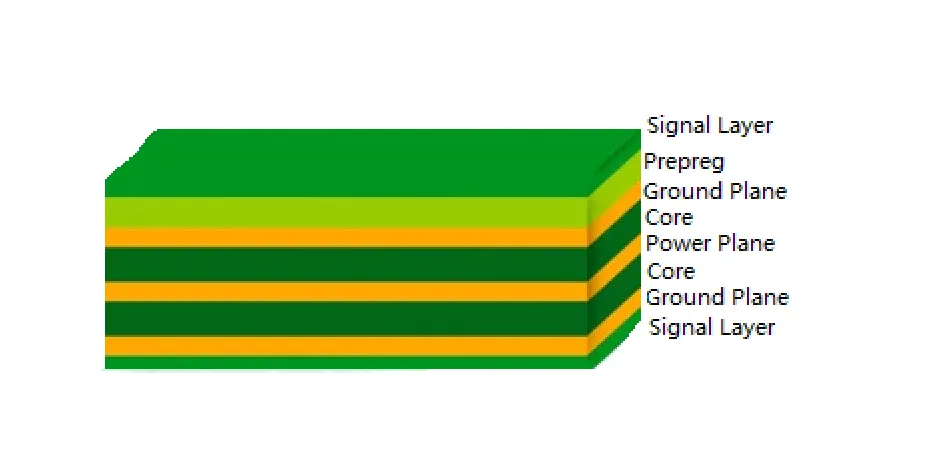
A symmetrical stackup is a layered structure in a multilayer PCB where the arrangement of conductive and dielectric layers is balanced around the board’s central axis. For instance, in an 8-layer PCB, the top four layers mirror the bottom four in terms of material thickness and copper distribution. This balance isn’t just aesthetic—it directly impacts the board’s electrical performance and physical stability.
Unlike asymmetrical stackups, where layer distribution can be uneven, symmetrical designs minimize issues like warping during manufacturing and ensure consistent electrical properties across the board. Whether you’re designing for high-speed applications or compact devices, understanding and implementing a symmetrical stackup can be a game-changer.
Why Choose a Symmetrical Stackup? Exploring the Advantages
Opting for a symmetrical stackup offers several key benefits, especially when designing complex or high-performance PCBs. Let’s break down the primary PCB symmetrical stackup advantages that make this approach a preferred choice for engineers.
1. Reduced Warpage and Mechanical Stress
During the manufacturing process, PCBs are exposed to heat and pressure, which can cause uneven expansion or contraction if the layer structure is unbalanced. A symmetrical stackup ensures that thermal expansion is uniform across the board, significantly reducing the risk of warpage. Studies suggest that asymmetrical designs can experience up to 30% more warpage compared to symmetrical ones under similar thermal conditions.
2. Improved Signal Integrity
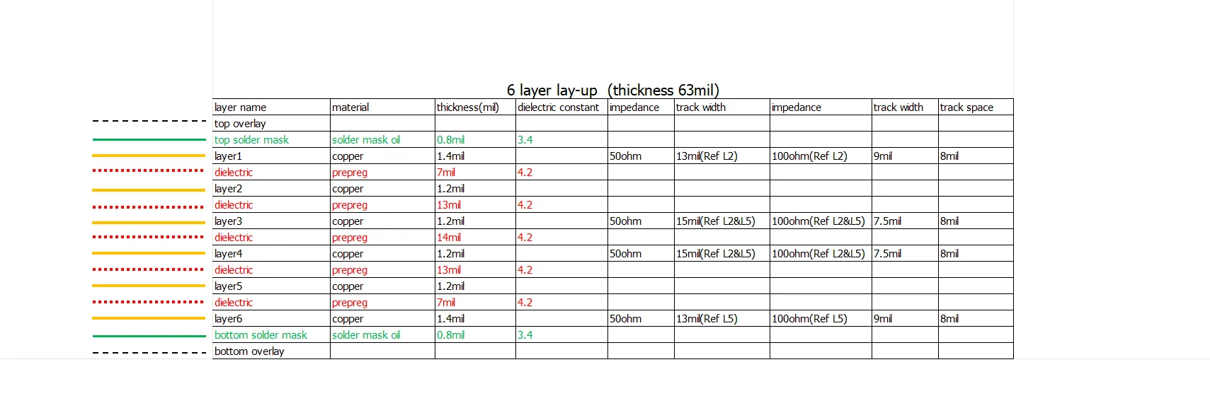
Signal integrity is crucial for high-speed designs, and a symmetrical stackup helps maintain consistent impedance across traces. By pairing signal layers with adjacent ground planes in a balanced manner, you can minimize crosstalk and electromagnetic interference (EMI). For example, in a 6-layer symmetrical stackup, placing ground planes on layers 2 and 5 ensures that signal layers on 1, 3, 4, and 6 have stable reference planes, reducing signal distortion.
3. Enhanced Manufacturability
Manufacturers prefer symmetrical stackups because they simplify the lamination process. Balanced layers lead to even pressure distribution during pressing, reducing the likelihood of defects like delamination. This not only improves yield rates but can also lower production costs by minimizing rework.
4. Better Thermal Management
A symmetrical design distributes heat more evenly across the PCB, preventing hotspots that could degrade components or affect performance. This is particularly important for power-intensive applications where thermal dissipation is a concern.
Symmetrical Stackup Design Rules: Building a Solid Foundation
Creating an effective symmetrical stackup isn’t just about mirroring layers—it requires careful planning and adherence to specific symmetrical stackup design rules. Below are essential guidelines to follow for optimal results.
1. Balance Copper Distribution
Ensure that copper density is roughly equal on corresponding layers. For example, if layer 1 has 1 oz copper, layer 8 (in an 8-layer board) should match it. Uneven copper distribution can lead to mechanical stress and affect impedance control.
2. Mirror Dielectric Thickness
The dielectric material between layers should have consistent thickness on both sides of the center. If the dielectric between layers 1 and 2 is 0.2 mm, the dielectric between layers 7 and 8 should be the same. This symmetry maintains uniform electrical properties and prevents manufacturing inconsistencies.
3. Place Power and Ground Planes Strategically
In a symmetrical stackup, power and ground planes should be positioned to mirror each other. For instance, in a 6-layer board, place ground on layer 2 and power on layer 5. This ensures that signal layers have nearby reference planes for better impedance matching, typically targeting values like 50 ohms for single-ended traces or 100 ohms for differential pairs.
4. Keep Layer Count Even When Possible
While not always feasible, using an even number of layers (e.g., 4, 6, 8) makes symmetry easier to achieve. Odd-layer counts can work but often require additional dummy layers to balance the structure, increasing cost and complexity.
5. Avoid Unnecessary Vias in Critical Areas
Excessive vias can disrupt the symmetry of copper distribution and introduce signal integrity issues. Plan via placement carefully, especially for high-speed signals, to maintain the stackup’s balance.
Symmetrical Stackup and Signal Integrity: Ensuring Reliable Performance
One of the standout benefits of a symmetrical stackup is its impact on symmetrical stackup signal integrity. High-speed designs, where signals operate at frequencies above 1 GHz, demand precise control over impedance, noise, and crosstalk. Here’s how a symmetrical stackup supports signal integrity and practical tips to optimize it.
Consistent Impedance Control
Impedance mismatches can cause signal reflections, leading to data errors in high-speed applications like USB 3.0 or PCIe. A symmetrical stackup ensures that traces on corresponding layers experience similar dielectric environments, maintaining consistent impedance. For example, a 50-ohm trace on layer 1 should have the same characteristics as a trace on layer 8 if the stackup is symmetrical.
Reduced Crosstalk and EMI
By placing ground planes adjacent to signal layers in a mirrored fashion, a symmetrical stackup minimizes crosstalk between traces. This is critical for differential pairs, where maintaining a 100-ohm impedance and minimal skew (e.g., less than 10 ps) is essential for protocols like HDMI or Ethernet.
Stable Return Paths
High-speed signals require uninterrupted return paths to avoid noise. In a symmetrical design, ground planes are evenly distributed, providing stable reference points for signals on outer and inner layers. This reduces loop inductance, which can otherwise degrade performance at speeds above 2.5 Gbps.
Symmetrical Stackup Manufacturing Process: From Design to Production
Understanding the symmetrical stackup manufacturing process is just as important as designing it. A well-planned stackup ensures smooth production and minimizes costly errors. Let’s walk through the key stages and considerations during manufacturing.
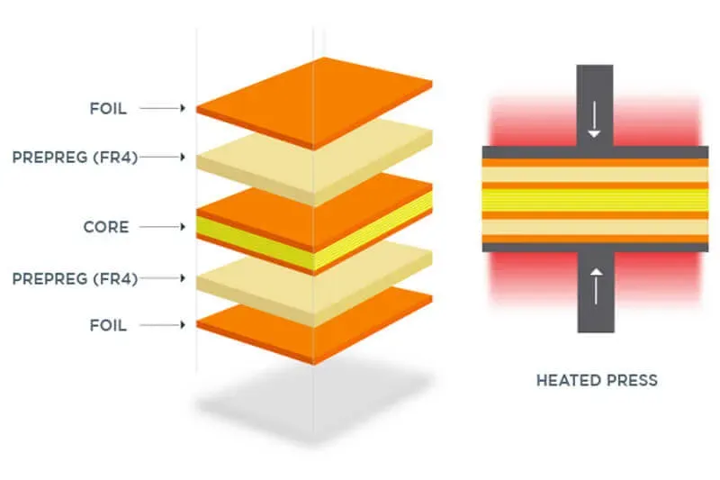
1. Material Selection
Choose dielectric materials with consistent properties (e.g., FR-4 with a dielectric constant of 4.2-4.5) to maintain symmetry. Ensure that core and prepreg thicknesses are uniform across mirrored layers to avoid lamination issues.
2. Layer Lamination
During lamination, manufacturers press the layers together under heat (around 180°C) and pressure. A symmetrical stackup ensures even force distribution, reducing the risk of voids or misalignment. Communicate your stackup design clearly in documentation to avoid errors at this stage.
3. Drilling and Via Formation
Drilling for vias must account for the symmetrical structure to maintain balance. Blind or buried vias, often used in high-density designs, should be placed to avoid disrupting copper symmetry. Ensure via aspect ratios (e.g., 8:1 for through-holes) are within manufacturing capabilities.
4. Quality Control
Manufacturers often use cross-sectional analysis to verify layer alignment and dielectric thickness post-lamination. Symmetrical stackups typically pass these checks more easily due to their balanced nature, but it’s still crucial to specify tight tolerances (e.g., ±10% for dielectric thickness) in your design files.
Common Challenges and How to Overcome Them
While symmetrical stackups offer numerous benefits, they aren’t without challenges. Here are a few common issues and solutions to ensure success.
Cost Constraints
Achieving perfect symmetry can sometimes require additional layers or materials, increasing costs. To mitigate this, prioritize symmetry in critical areas (e.g., high-speed signal layers) while allowing minor deviations in less sensitive regions.
Design Complexity
For intricate designs with mixed-signal requirements, maintaining symmetry can be tricky. Use simulation tools to model signal behavior and adjust layer placement iteratively until balance is achieved without compromising functionality.
Manufacturer Limitations
Not all fabrication houses can handle highly symmetrical stackups with tight tolerances. Partner with a reliable manufacturer and review their capabilities (e.g., minimum dielectric thickness, via types) before finalizing your design.
Conclusion: Elevate Your PCB Designs with Symmetrical Stackups
Mastering symmetrical stackups is a vital skill for any PCB designer aiming to create high-performance, reliable boards. From reducing warpage and enhancing signal integrity to streamlining the manufacturing process, the benefits of a balanced layer structure are undeniable. By following the symmetrical stackup design rules outlined in this guide and leveraging the PCB symmetrical stackup advantages, you can tackle even the most demanding projects with confidence.
Whether you’re optimizing for symmetrical stackup signal integrity in high-speed applications or ensuring a smooth symmetrical stackup manufacturing process, a thoughtful approach to stackup design pays off in the long run. Start implementing these principles in your next project, and watch as your PCBs achieve new levels of performance and reliability.


