ALLPCB


Fine line PCB manufacturing is a critical process for creating high-density, high-performance circuit boards used in advanced electronics. However, it comes with unique challenges like achieving precision in trace widths, ensuring signal integrity, and managing material properties. In this comprehensive guide, we’ll explore the fine line PCB manufacturing process, dive into common obstacles, and provide practical solutions to help engineers and designers achieve optimal results. Whether you’re tackling fine line PCB fabrication or seeking advanced PCB etching techniques, this blog offers actionable insights to elevate your projects.
What Is Fine Line PCB Manufacturing?
Fine line PCB manufacturing refers to the production of printed circuit boards with extremely narrow trace widths and spacing, typically ranging from 2 to 5 mils (0.002 to 0.005 inches). These boards are essential for modern electronics, such as smartphones, medical devices, and automotive systems, where space is limited, and performance demands are high. The process requires cutting-edge technologies like laser direct imaging and specialized material selection to ensure precision and reliability.
In the following sections, we’ll break down the fine line PCB fabrication process, highlight key challenges, and share proven solutions to help you master this intricate craft.
Understanding the Fine Line PCB Manufacturing Process
The fine line PCB manufacturing process involves several intricate steps to achieve the desired precision. Each stage, from design to final testing, plays a crucial role in ensuring the board meets strict performance standards. Let’s walk through the core steps involved:
- Design and Layout: The process begins with creating a detailed digital design of the PCB, specifying trace widths, spacing, and layer stack-up. Software tools help optimize the layout for signal integrity and manufacturability.
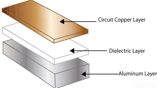
- Material Selection: Choosing the right substrate and copper thickness is vital for fine line PCBs. Materials must support high-frequency signals and withstand the manufacturing process without degrading.
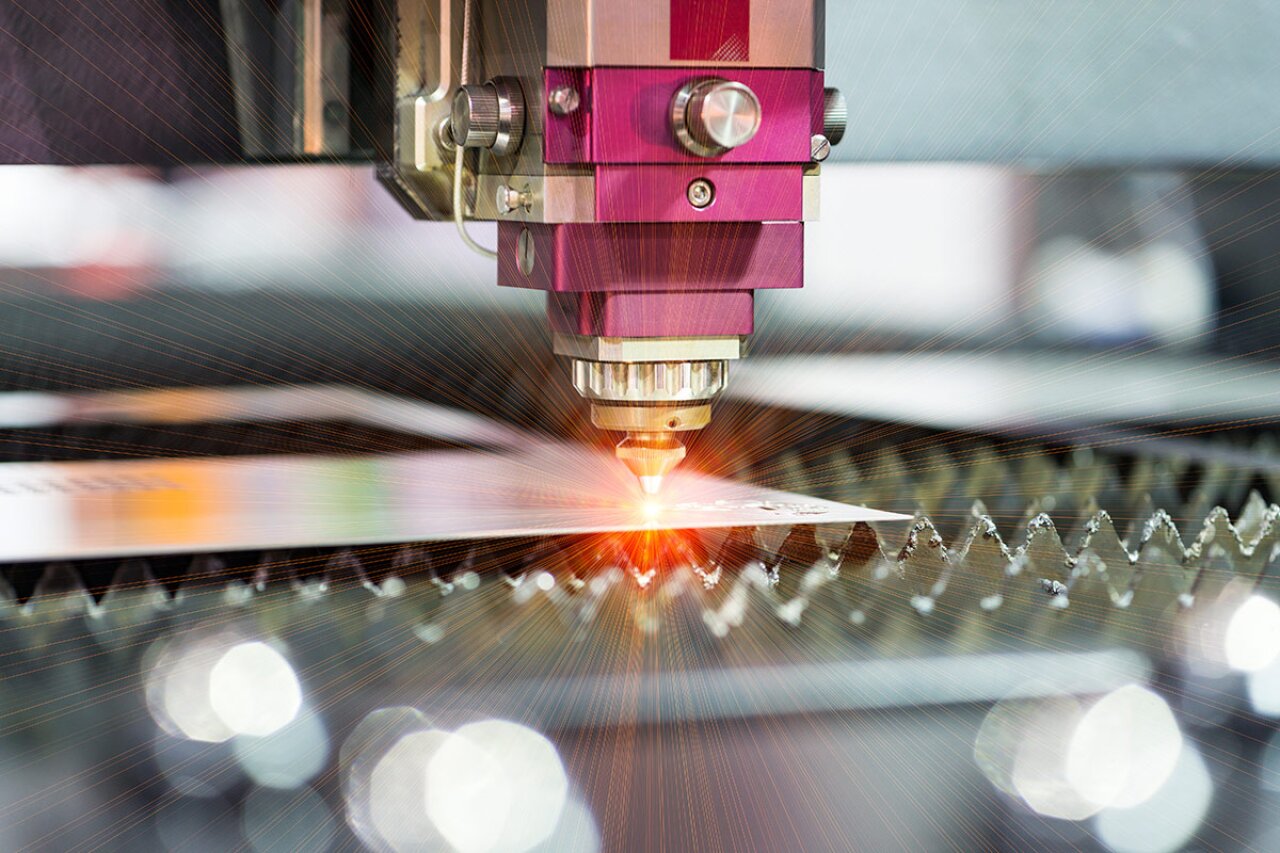
- Imaging: Advanced techniques like laser direct imaging (LDI) transfer the design onto the board with exceptional accuracy, ensuring fine traces are precisely defined.
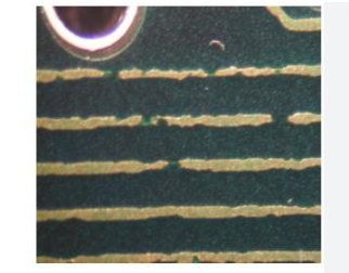
- Etching: PCB etching techniques remove excess copper to form the narrow traces. This step requires tight control to avoid over-etching or under-etching.
- Lamination and Drilling: For multilayer boards, layers are stacked and bonded under heat and pressure. Microvias are drilled to connect layers, often using laser technology for precision.
- Plating and Finishing: Copper plating strengthens traces and vias, while surface finishes like ENIG (Electroless Nickel Immersion Gold) protect against corrosion and ensure solderability.
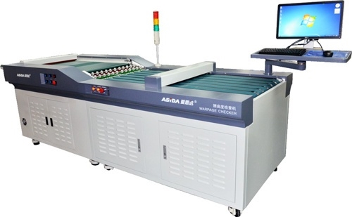
- Testing: Rigorous electrical and visual inspections verify trace continuity, spacing, and overall board quality.
Key Challenges in Fine Line PCB Fabrication
While fine line PCB fabrication enables compact and high-performance designs, it introduces several challenges that can impact yield and reliability. Below are some of the most common obstacles engineers face:
1. Achieving Precision in Trace Widths and Spacing
With trace widths as narrow as 2 mils, even slight deviations during imaging or etching can lead to open circuits or shorts. Maintaining consistent spacing is equally critical to prevent signal crosstalk, especially in high-density designs.
2. Signal Integrity Issues
Fine line PCBs often handle high-frequency signals, making them susceptible to impedance mismatches and signal loss. For example, a trace width variation of just 0.5 mils can alter impedance by several ohms, disrupting signal performance at frequencies above 1 GHz.
3. Material Limitations
Standard PCB materials may not support the thermal and mechanical stresses of fine line fabrication. High-frequency applications often require low-loss dielectrics, which can be costly and harder to process.
4. Etching Accuracy
Traditional subtractive etching struggles to produce ultra-fine traces without over-etching, which can weaken traces or cause breaks. Undercutting—where etchants remove material beneath the resist—further complicates the process.
5. Manufacturing Equipment Limitations
Not all fabrication facilities are equipped with the advanced tools needed for fine line production, such as high-resolution imaging systems or laser drilling machines. This can lead to inconsistent results or higher costs.
Solutions for Mastering Fine Line PCB Manufacturing
Overcoming the challenges of fine line PCB manufacturing requires a combination of advanced technologies, optimized processes, and careful material selection. Here are actionable solutions to address the issues outlined above:
1. Leverage Laser Direct Imaging (LDI) for Precision
Laser direct imaging is a game-changer for fine line PCB fabrication. Unlike traditional photolithography, LDI uses a laser to directly expose the photoresist, achieving resolutions down to 1 mil or less. This eliminates the need for physical masks, reducing alignment errors and enabling tighter tolerances. By adopting LDI, manufacturers can consistently produce trace widths and spacing with deviations of less than 0.1 mil.
2. Optimize PCB Etching Techniques
Advanced PCB etching techniques, such as semi-additive processes (SAP), offer better control over fine line formation. In SAP, a thin layer of copper is initially deposited, and traces are built up through selective plating rather than etching away large amounts of material. This method reduces undercutting and allows for traces as narrow as 15 microns (0.6 mils). Additionally, using high-quality etchants and precise process controls can minimize over-etching risks.
3. Focus on Material Selection for Fine Line PCBs
Choosing the right materials is critical for fine line PCBs, especially for high-frequency or high-speed applications. Low-loss substrates like PTFE-based laminates or high-Tg FR-4 variants can maintain signal integrity at frequencies up to 10 GHz. Copper foils with lower surface roughness (e.g., 0.5 μm RMS) also reduce signal loss and improve etching accuracy. When selecting materials, consider dielectric constant (Dk) values—typically between 2.2 and 3.5 for high-frequency designs—and thermal expansion properties to prevent delamination during manufacturing.
4. Enhance Signal Integrity with Design and Simulation
To mitigate signal integrity issues, use simulation tools during the design phase to predict impedance and signal behavior. For instance, maintaining a controlled impedance of 50 ohms for high-speed traces often requires precise stack-up design and dielectric thickness control within 0.1 mil. Additionally, incorporating ground planes and minimizing trace length variations can reduce crosstalk and electromagnetic interference (EMI).
5. Partner with Advanced Manufacturing Facilities
Work with fabrication partners equipped with state-of-the-art tools for fine line production. Facilities with LDI systems, laser drilling capabilities for microvias (down to 0.1 mm diameter), and automated optical inspection (AOI) can ensure consistent quality. Collaborating with experienced manufacturers also provides access to process expertise, reducing trial-and-error costs.
Advanced Tips for Fine Line PCB Success
Beyond the core solutions, consider these advanced strategies to further enhance your fine line PCB projects:
- Adopt HDI Technology: High-density interconnect (HDI) techniques, such as microvias and buried vias, complement fine line designs by increasing routing density without expanding board size.
- Use Automated Inspection: Automated optical inspection (AOI) and electrical testing detect defects like trace breaks or shorts early in the process, ensuring yields remain high.
- Iterate Designs: Prototype and test multiple iterations of your fine line PCB to refine trace layouts and material choices before full-scale production.
- Control Environmental Factors: Maintain strict cleanroom conditions during fabrication to prevent dust or contaminants from affecting fine traces, which can cause defects at scales below 3 mils.
Why Fine Line PCB Manufacturing Matters in 2025
As of 2025, the demand for fine line PCBs continues to grow with the rise of 5G technology, electric vehicles, and IoT devices. These applications require compact boards with trace widths below 3 mils to support faster data rates (up to 100 Gbps in some 5G systems) and higher component densities. Mastering fine line fabrication is no longer optional—it’s a necessity for staying competitive in the electronics industry.
Moreover, advancements in manufacturing technologies, such as improved laser systems and semi-additive processes, are making fine line production more accessible. By addressing challenges like etching precision and material compatibility, engineers can unlock the full potential of next-generation electronics.

Conclusion: Taking Your Fine Line PCB Projects to the Next Level
Fine line PCB manufacturing is a complex but rewarding process that enables the creation of cutting-edge electronics. By understanding the intricacies of the fine line PCB manufacturing process, addressing challenges like precision and signal integrity, and implementing solutions such as laser direct imaging and optimized material selection for fine line PCBs, you can achieve exceptional results. Whether you’re refining PCB etching techniques or exploring advanced fabrication methods, the strategies outlined in this guide provide a solid foundation for success.