 ALLPCB


In the fast-evolving world of artificial intelligence (AI), the demand for high-performance hardware is at an all-time high. AI accelerator PCBs (Printed Circuit Boards) are at the heart of this revolution, powering the complex computations needed for machine learning and deep learning tasks. However, manufacturing these advanced boards comes with significant challenges, especially when it comes to High-Density Interconnect (HDI) technology. This blog dives deep into the intricacies of AI accelerator PCB HDI manufacturing, exploring key hurdles like microvia fabrication, laser drilling, and fine-line etching, while also highlighting advanced PCB manufacturing techniques to overcome them.
Whether you're an engineer designing cutting-edge AI hardware or a manufacturer looking to optimize production, this guide offers practical insights and solutions to help you navigate the complexities of HDI PCB manufacturing for AI applications.
What Are AI Accelerator PCBs and Why Is HDI Crucial?
AI accelerators are specialized hardware designed to handle the massive parallel processing required for AI workloads. These include GPUs, TPUs, and custom ASICs (Application-Specific Integrated Circuits) that power everything from data centers to edge devices. The PCBs that support these components must accommodate high-speed signals, dense component layouts, and efficient power delivery—all while maintaining a compact form factor.
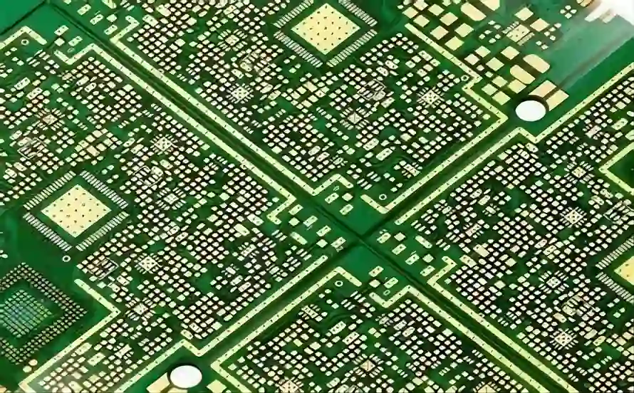
This is where High-Density Interconnect (HDI) technology becomes essential. HDI PCBs allow for tighter component placement and shorter signal paths by using smaller vias, finer traces, and multiple layers. For AI accelerator PCBs, HDI enables higher performance by reducing signal loss and crosstalk, which are critical for maintaining data integrity at speeds often exceeding 10 Gbps. However, achieving these benefits requires overcoming significant manufacturing challenges, which we’ll explore in detail below.
Key Challenges in AI Accelerator PCB HDI Manufacturing
Manufacturing HDI PCBs for AI accelerators is no easy task. The need for precision, reliability, and scalability pushes the limits of current fabrication technologies. Below are some of the most pressing challenges faced in AI accelerator PCB HDI manufacturing.
1. Microvia Fabrication for AI PCBs
Microvias are tiny holes (typically less than 150 microns in diameter) used to connect layers in HDI PCBs. They are critical for achieving the high-density routing needed in AI accelerator boards. However, microvia fabrication for AI PCBs presents several hurdles:
- Precision and Reliability: Microvias must be perfectly aligned to avoid signal disruptions. A misalignment of even 10 microns can lead to connection failures, especially in boards with 10 or more layers.
- Thermal Stress: AI accelerators generate significant heat, often exceeding 100°C during operation. This can cause microvias to crack or delaminate if not fabricated with high-quality materials and processes.
- Cost vs. Scalability: Producing reliable microvias at scale increases manufacturing costs, as it requires advanced equipment and strict quality control.
To address these issues, manufacturers often rely on sequential lamination processes and high-performance dielectric materials that can withstand thermal stress. Ensuring microvia reliability is crucial for maintaining the performance of AI hardware over time.
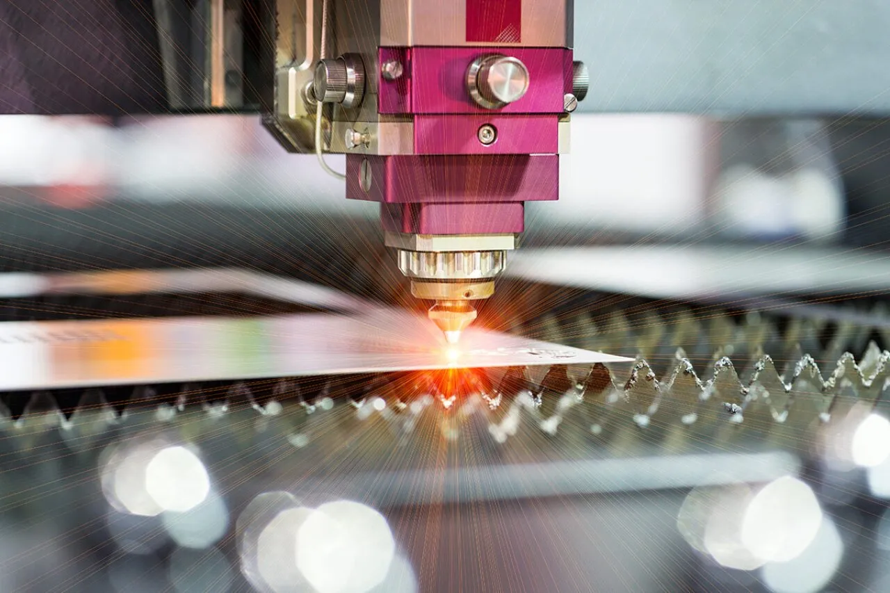
2. Laser Drilling Challenges in AI PCBs
Laser drilling is the go-to method for creating microvias in HDI PCBs due to its precision and ability to handle small diameters. For AI accelerator PCBs, where via sizes can be as small as 50 microns, laser drilling is indispensable. However, it comes with its own set of challenges:
- Material Variability: Different PCB materials, such as FR-4 or high-frequency laminates, respond differently to laser drilling. Inconsistent drilling can lead to uneven via walls or debris buildup, affecting signal integrity.
- Depth Control: Achieving uniform depth in stacked microvias (used in multi-layer HDI boards) is difficult. Over-drilling can damage underlying layers, while under-drilling can result in poor connections.
- High Equipment Costs: Advanced laser drilling systems, capable of handling the precision needed for AI PCBs, are expensive and require regular maintenance to ensure consistent performance.
Manufacturers are tackling these challenges by adopting CO2 and UV laser systems, which offer better control over drilling depth and minimize thermal damage to surrounding materials. Additionally, automated inspection systems help detect defects early in the process.
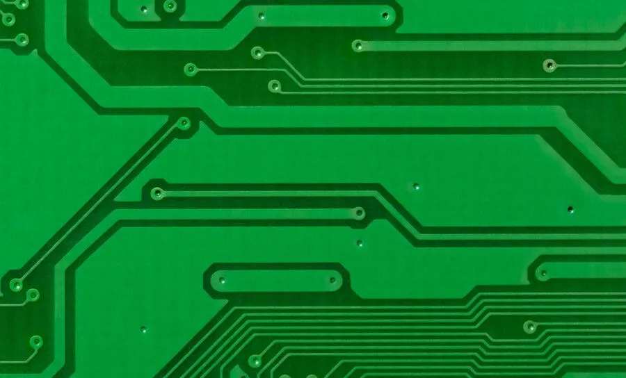
3. Fine-Line Etching for AI PCB Density
Fine-line etching is the process of creating narrow copper traces (often less than 50 microns wide) on a PCB to support high-density layouts. In AI accelerator PCBs, fine-line etching is critical for routing high-speed signals with minimal interference. However, achieving consistent fine lines poses several challenges:
- Trace Uniformity: Variations in etching can lead to uneven trace widths, causing impedance mismatches. For high-speed signals (e.g., 25 Gbps or higher), even a 5% deviation in trace width can degrade performance.
- Signal Integrity: Narrow traces are more susceptible to crosstalk and electromagnetic interference (EMI), which are major concerns in densely packed AI boards.
- Manufacturing Limits: Traditional etching processes struggle to achieve lines finer than 30 microns without defects like undercutting or over-etching.
To overcome these issues, advanced photoresist materials and direct imaging technologies are used to improve etching precision. Additionally, impedance control testing during production ensures that fine traces meet the strict requirements of AI applications.
Advanced PCB Manufacturing Techniques for AI Accelerators
While the challenges of AI accelerator PCB HDI manufacturing are significant, cutting-edge techniques and technologies are helping manufacturers meet the demands of this rapidly growing field. Below are some of the most effective advanced PCB manufacturing techniques being used today.
1. Sequential Build-Up (SBU) for HDI Layers
Sequential Build-Up (SBU) is a cornerstone of HDI PCB manufacturing. This process involves adding layers of dielectric and copper one at a time, allowing for the integration of microvias and fine traces at each stage. For AI accelerator PCBs, SBU offers several benefits:
- Higher Density: SBU enables the creation of boards with 12 or more layers, accommodating the complex routing needed for AI hardware.
- Improved Signal Performance: By minimizing via stub lengths, SBU reduces signal reflections and supports high-speed data transfer.
- Flexibility: SBU allows manufacturers to customize layer configurations based on the specific requirements of an AI accelerator design.
This technique requires precise control over lamination and alignment, but it’s a proven method for achieving the density and performance needed in AI applications.
2. Via-in-Pad Technology for Space Efficiency
Via-in-Pad technology places microvias directly under component pads, freeing up valuable board space for additional routing. This is especially useful in AI accelerator PCBs, where fine-pitch components like BGAs (Ball Grid Arrays) are common. Benefits include:
- Reduced Board Size: Via-in-Pad can shrink PCB footprints by up to 30%, critical for compact AI devices.
- Better Signal Routing: Direct connections under pads shorten signal paths, reducing latency and improving performance.
However, Via-in-Pad requires advanced laser drilling and plating techniques to ensure reliable connections without voids or defects. Automated optical inspection (AOI) is often used to verify quality during production.
3. High-Performance Materials for Thermal and Electrical Needs
AI accelerators push PCBs to their thermal and electrical limits. Using high-performance materials is an advanced technique that addresses these demands:
- Low-Loss Dielectrics: Materials with low dielectric constants (Dk) and dissipation factors (Df) minimize signal loss at high frequencies, supporting speeds above 20 Gbps.
- High-Tg Laminates: Laminates with a high glass transition temperature (Tg) resist deformation under heat, ensuring reliability in AI systems that operate at elevated temperatures.
- Thermal Conductive Substrates: These materials dissipate heat efficiently, preventing hotspots that could damage components or degrade performance.
Selecting the right materials is a critical step in AI accelerator PCB design and manufacturing, as it directly impacts both performance and longevity.
4. Automated Inspection and Testing for Quality Assurance
With the tight tolerances required in AI accelerator PCB HDI manufacturing, automated inspection and testing are indispensable. Techniques like Automated Optical Inspection (AOI) and X-ray imaging detect defects in microvias and fine traces before they become costly failures. Electrical testing, such as Time-Domain Reflectometry (TDR), ensures impedance values stay within a narrow range (e.g., ±10% of 50 ohms for high-speed lines).
These advanced quality control measures help manufacturers catch issues early, reducing scrap rates and ensuring that every board meets the stringent demands of AI applications.
How to Optimize AI Accelerator PCB Manufacturing
For engineers and manufacturers looking to streamline AI accelerator PCB HDI manufacturing, consider the following best practices:
- Collaborate Early: Work closely with your PCB fabrication partner during the design phase to align on material choices, layer stack-ups, and manufacturing capabilities.
- Prioritize Simulation: Use signal integrity and thermal simulation tools to predict performance issues before production, minimizing costly redesigns.
- Focus on Scalability: Design with manufacturing in mind, choosing processes and materials that can be scaled for high-volume production without sacrificing quality.
- Stay Updated: Keep abreast of advancements in laser drilling, fine-line etching, and other technologies to leverage the latest solutions for HDI challenges.
By adopting these strategies, you can navigate the complexities of AI accelerator PCB manufacturing and deliver high-performance boards that meet the demands of modern AI systems.
Conclusion: Mastering HDI Challenges for AI Accelerator PCBs
The rise of AI technology has placed unprecedented demands on PCB design and manufacturing. AI accelerator PCBs, with their need for high-density interconnects, push the boundaries of what’s possible in terms of microvia fabrication, laser drilling, and fine-line etching. While these challenges are significant, advanced PCB manufacturing techniques like sequential build-up, Via-in-Pad technology, and the use of high-performance materials offer practical solutions to achieve the performance and reliability required.
At ALLPCB, we’re committed to helping engineers and manufacturers overcome the hurdles of AI accelerator PCB HDI manufacturing. By leveraging cutting-edge technologies and maintaining a focus on precision and quality, we support the development of next-generation AI hardware that powers innovation across industries. Whether you’re working on data center solutions or edge AI devices, mastering these manufacturing challenges is the key to staying ahead in this competitive field.


