 ALLPCB


In the world of PCB design, ensuring signal integrity is crucial, especially for high-speed applications. One of the key factors that directly affects signal integrity is the trace width, often referred to as line width. So, how does line width impact signal integrity? Simply put, the width of a trace influences the impedance, current-carrying capacity, and potential for signal reflection or interference in a circuit. A poorly chosen trace width can lead to impedance mismatch, signal degradation, and even complete system failure in high-speed PCB designs.
In this comprehensive guide, we'll dive deep into the relationship between trace width and signal integrity, exploring concepts like impedance control, signal reflection, and best practices for high-speed PCB design. Whether you're a seasoned engineer or a beginner, this blog will provide actionable insights to optimize your designs and avoid common pitfalls.
What Is Signal Integrity and Why Does It Matter?
Signal integrity refers to the ability of an electrical signal to maintain its quality as it travels through a printed circuit board (PCB). In other words, the signal should reach its destination without distortion, noise, or loss of data. Poor signal integrity can result in errors, delays, or system malfunctions, which are especially problematic in high-speed designs where signals switch at frequencies of hundreds of megahertz or even gigahertz.
Trace width plays a pivotal role in maintaining signal integrity. It affects how much current a trace can carry, the resistance of the trace, and most importantly, the characteristic impedance. When the impedance isn't properly matched, signals can reflect back along the trace, causing interference and data errors. As we explore this topic, you'll see how trace width ties directly to these critical aspects of PCB performance.

How Trace Width Affects Signal Integrity in PCB Design
The width of a trace on a PCB isn't just about fitting it onto the board; it has a direct impact on electrical performance. Let's break down the key ways trace width influences signal integrity.
1. Impedance Control and Matching
Characteristic impedance is a measure of how much opposition a trace offers to the flow of an alternating current signal. For high-speed signals, maintaining a consistent impedance (often 50 ohms or 75 ohms, depending on the application) is essential to prevent signal reflection. Trace width is one of the primary factors determining this impedance.
A narrower trace generally has higher impedance because it has less copper to conduct the signal, while a wider trace lowers the impedance. If the impedance of the trace doesn't match the source or load impedance, part of the signal reflects back, causing noise and potential data loss. For instance, in a high-speed USB design operating at 480 Mbps, a trace width deviation of just a few mils can shift the impedance outside the acceptable range of 90 ohms ±15%, leading to signal integrity issues.
To calculate the right trace width for a specific impedance, designers use formulas or simulation tools based on the PCB stack-up, dielectric constant of the material (often around 4.2 for FR-4), and trace thickness (typically 1 oz copper, or 1.4 mils). For example, a 50-ohm impedance trace on a standard two-layer board might require a width of approximately 6-8 mils, depending on the board's specifics.
2. Signal Reflection Due to Impedance Mismatch
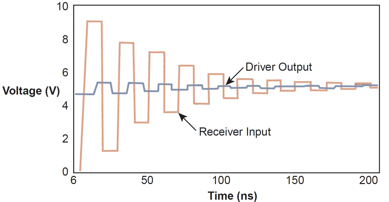
When there's an impedance mismatch caused by incorrect trace width, signal reflection occurs. This happens because the signal encounters a sudden change in impedance, sending a portion of the energy back toward the source. Reflections can interfere with the original signal, creating noise or "ringing" that distorts data.
For high-speed designs like DDR memory interfaces operating at 1 GHz or more, even a small reflection can cause timing errors. Adjusting trace width to match the required impedance minimizes these reflections, ensuring cleaner signal transmission.
3. Current-Carrying Capacity and Heat Dissipation
Trace width also determines how much current a trace can safely carry without overheating. A trace that's too narrow for the current it carries will heat up, potentially damaging the PCB or altering the signal's behavior due to increased resistance. For high-speed signals, this added resistance can also degrade the signal's amplitude, leading to errors.
For example, a trace carrying 1 amp of current on a standard 1 oz copper layer typically needs a width of at least 20 mils to avoid excessive heat buildup (based on IPC-2221 standards). If the trace is narrower, the temperature rise could exceed 10°C, impacting nearby components and signal integrity.
4. Crosstalk and Electromagnetic Interference (EMI)
In high-speed PCB designs, traces placed close together can interfere with each other through crosstalk, where a signal on one trace induces noise on a neighboring trace. Wider traces can reduce resistance and improve signal strength, but they may also increase the capacitive coupling between traces if not spaced properly.
To mitigate crosstalk, designers often balance trace width with adequate spacing (typically 3 times the trace width for critical signals) and use ground planes to shield signals. For instance, in a 10 Gbps Ethernet design, maintaining a trace width of 5 mils with a spacing of 15 mils can help reduce crosstalk while keeping impedance in check.
Trace Width Effects in High-Speed PCB Design
High-speed PCB design amplifies the importance of trace width because signals switch faster, leaving less room for error. At frequencies above 100 MHz, effects like signal reflection, crosstalk, and propagation delay become more pronounced. Here's how trace width specifically impacts high-speed applications.
Propagation Delay and Timing
In high-speed designs, the time it takes for a signal to travel along a trace—known as propagation delay—must be carefully managed. Trace width, along with the dielectric material, affects the speed of signal propagation. A wider trace can slightly reduce delay due to lower resistance, but it must still match the impedance requirements to avoid reflections that disrupt timing.
For example, in a PCIe 3.0 design operating at 8 GT/s, timing margins are incredibly tight. A trace width mismatch could introduce a delay of just a few picoseconds, enough to cause data errors.
Skin Effect at High Frequencies
At high frequencies, the skin effect causes current to flow primarily on the surface of the conductor rather than through its entire cross-section. This increases the effective resistance of the trace, especially if it's too narrow. Wider traces can help mitigate the skin effect by providing more surface area for current flow, but they must be balanced with impedance needs.
Best Practices for Optimizing Trace Width in PCB Design
Now that we understand the impact of trace width on signal integrity, let's look at practical steps to optimize it for your designs, especially in high-speed applications.
1. Use Impedance Calculators and Simulation Tools
Before routing traces, use impedance calculators or simulation software to determine the correct trace width for your target impedance. These tools account for factors like board material, layer stack-up, and trace thickness. For a 50-ohm trace on FR-4 material with a 1.6 mm board thickness, the calculator might suggest a width of 6.5 mils—always verify with your manufacturer's capabilities.
2. Follow Design Standards and Guidelines
Adhere to industry standards like IPC-2221 for trace width based on current and temperature rise. Additionally, follow specific guidelines for high-speed protocols (e.g., USB, HDMI, PCIe) that often specify impedance and trace width tolerances.
3. Maintain Consistent Trace Widths
Avoid sudden changes in trace width along a signal path, as this can cause impedance discontinuities and reflections. If a width change is necessary (e.g., transitioning to a connector), use a gradual taper to minimize disruption.
4. Incorporate Ground Planes
A solid ground plane beneath signal traces helps maintain consistent impedance and reduces EMI. Ensure the ground plane is unbroken under critical high-speed traces, as voids or cuts can alter impedance and degrade signal integrity.
5. Test and Validate Designs
After designing, use tools like time-domain reflectometry (TDR) to measure impedance along traces and identify mismatches. Prototyping and testing with real hardware can also reveal signal integrity issues tied to trace width before full production
Common Mistakes to Avoid with Trace Width in PCB Design
Even experienced designers can make errors when dealing with trace width. Here are some pitfalls to watch out for:
- Underestimating Current Needs: Choosing a trace width that's too narrow for the current can lead to overheating and signal loss.
- Ignoring Impedance Matching: Failing to calculate the correct width for impedance can cause reflections, especially in high-speed designs.
- Inconsistent Routing: Varying trace widths or poor spacing can introduce noise and crosstalk between signals.
- Overlooking Manufacturing Limits: Designing traces narrower than what your manufacturer can reliably produce (often below 3-4 mils) can lead to defects.
Conclusion: Mastering Trace Width for Better Signal Integrity
Trace width is a fundamental aspect of PCB design that directly impacts signal integrity, especially in high-speed applications. By understanding how trace width affects impedance, signal reflection, current capacity, and crosstalk, you can make informed decisions to optimize your designs. Use the right tools to calculate trace widths, follow industry standards, and test your layouts to ensure reliable performance.
Whether you're working on a simple circuit or a complex high-speed system, paying attention to trace width effects will help you avoid signal integrity issues and deliver robust, efficient PCBs. With these insights and best practices, you're well-equipped to tackle the challenges of modern PCB design and achieve success in your projects.


