 ALLPCB


In the world of printed circuit boards (PCBs), layer count plays a significant role in determining the maximum achievable size of a board. Simply put, as the number of layers in a PCB increases, the potential for larger board sizes often decreases due to manufacturing constraints, signal integrity concerns, and thermal management challenges. However, with advancements in multilayer PCB design and high-density interconnect (HDI) technology, engineers can push these boundaries to meet the demands of complex electronics. In this comprehensive guide, we’ll explore how PCB layer count and size interact, dive into the intricacies of multilayer PCB design, and discuss solutions like HDI PCB technology to maximize performance while maintaining signal integrity in multilayer PCBs.
Understanding PCB Layer Count and Its Role in Design
A PCB’s layer count refers to the number of conductive copper layers embedded within or on the surface of the board, separated by insulating materials. These layers can range from a single layer in simple designs to over 30 layers in advanced applications like telecommunications or aerospace systems. Each layer serves a purpose, whether it’s for routing signals, providing power, or acting as a ground plane.
The layer count directly impacts the complexity and functionality of a PCB. More layers allow for denser routing and integration of components, which is essential for modern electronics. However, as the layer count increases, so do the challenges related to size, manufacturing precision, and performance. Let’s break down how layer count influences the maximum achievable PCB size and why it matters for engineers working on intricate designs.
How Layer Count Affects Maximum PCB Size
The relationship between PCB layer count and size is not always straightforward, as it depends on several factors, including manufacturing capabilities, material properties, and design requirements. Below, we explore the key ways in which layer count impacts the maximum size of a PCB.
1. Manufacturing Constraints and Panel Size Limitations
During PCB fabrication, boards are typically produced on large panels, which are then cut into individual units. The size of these panels is limited by the equipment used in advanced PCB fabrication processes. For multilayer boards with high layer counts (e.g., 12 or more), manufacturers often face challenges in maintaining uniformity across larger panels due to issues like warpage, thermal expansion, and alignment precision between layers.
For instance, a standard panel size might be 18 x 24 inches, but as layer count increases, the risk of defects rises, especially for larger boards. This often forces manufacturers to limit the maximum size of high-layer-count PCBs to ensure quality. In practical terms, a 4-layer board might achieve a size of up to 20 x 16 inches with ease, while a 16-layer board could be restricted to 12 x 10 inches or smaller to maintain structural integrity during production.
2. Material Thickness and Weight Considerations
Each additional layer adds to the overall thickness and weight of the PCB. A typical 2-layer board might be around 1.6 mm thick, while a 12-layer board could exceed 3 mm, depending on the dielectric material and copper thickness used. As the board gets thicker, it becomes more challenging to handle larger sizes due to mechanical stress and potential bending or cracking during assembly and operation.
Moreover, thicker boards require more robust materials, which can increase costs and limit the maximum size due to availability and handling constraints. Engineers must balance layer count with size to ensure the board remains practical for its intended application.
3. Thermal Management Challenges
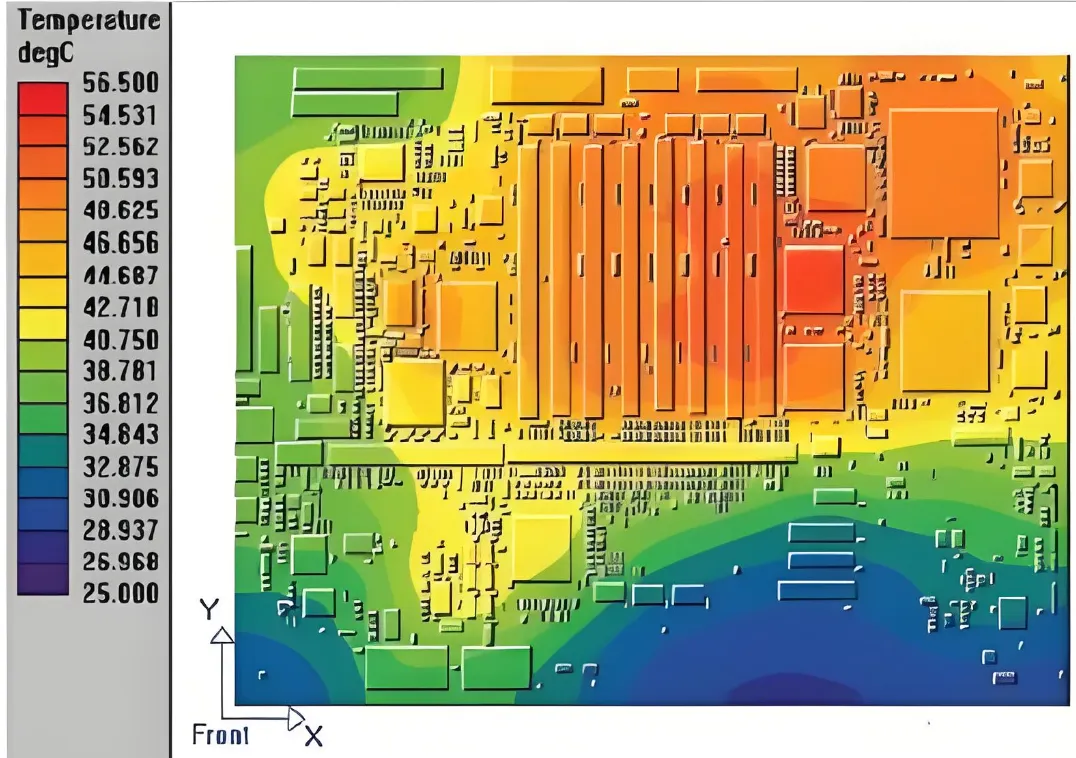
High layer counts often mean more components and power dissipation, leading to increased heat generation. Larger PCBs with many layers can struggle with heat dissipation, as the inner layers trap heat, creating thermal hotspots. This issue becomes more pronounced in larger boards, where heat has a longer path to escape to the edges or through vias.
To mitigate this, designers may need to incorporate thermal vias or heat sinks, which can reduce the usable area for routing and components, effectively limiting the maximum size. For example, a 10-layer PCB designed for a high-power application might need to stay under 10 x 8 inches to ensure proper heat distribution without additional cooling mechanisms.
Multilayer PCB Design: Balancing Complexity and Size
Multilayer PCB design is a powerful approach to creating compact, high-performance electronics, but it requires careful planning to manage size constraints. Here are some strategies to optimize designs while addressing the impact of layer count on board size.
1. Layer Stacking and Impedance Control
In multilayer designs, the arrangement of layers (known as the stack-up) is critical for maintaining signal integrity in multilayer PCBs. For example, placing ground planes adjacent to signal layers can reduce electromagnetic interference (EMI) and crosstalk. However, achieving the desired impedance—often around 50 ohms for high-speed signals—requires precise control over layer thickness and dielectric constants, which can be challenging in larger boards with many layers.
For a 6-layer PCB, a common stack-up might include two signal layers on the top and bottom, with ground and power planes in the middle. As layer count increases to 12 or more, maintaining consistent impedance across a larger area becomes harder due to material variations, potentially limiting the board’s size.
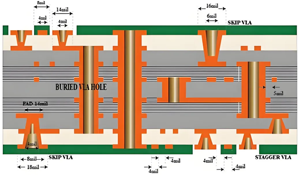
2. Via Types and Routing Density
Vias are essential for connecting layers in a multilayer PCB, but they also impact size and routing efficiency. Through-hole vias, which pass through all layers, consume more space and can restrict routing on larger boards. Blind and buried vias, often used in HDI PCB designs, save space by connecting only specific layers, allowing for higher density and potentially larger board sizes without sacrificing performance.
For instance, a 16-layer PCB using standard through-hole vias might be limited to a smaller size due to routing congestion, while the same design with HDI techniques could achieve a larger footprint by optimizing via placement.
HDI PCB Technology: Pushing the Limits of Size and Layer Count
HDI PCB technology, or High-Density Interconnect, is a game-changer for engineers looking to maximize PCB size and layer count without compromising performance. HDI designs use microvias (vias with diameters less than 0.15 mm) and finer traces to achieve higher component density and better signal integrity.
Benefits of HDI for Larger Multilayer PCBs
HDI technology allows for more layers in a thinner profile, reducing overall board thickness and enabling larger sizes. For example, an HDI board with 20 layers might achieve a thickness of only 2.5 mm, compared to 4 mm for a traditional multilayer board, making it easier to handle larger dimensions without mechanical issues.
Additionally, HDI improves signal integrity in multilayer PCBs by minimizing signal loss and crosstalk through shorter interconnects and better layer stacking. This is particularly important for high-frequency applications, where signal speeds can exceed 5 GHz, and maintaining integrity over larger board areas is critical.
Applications of HDI in Large PCBs
HDI technology is widely used in industries like telecommunications, automotive, and medical devices, where large, complex PCBs with high layer counts are common. For instance, a telecom server board might measure 18 x 12 inches with 24 layers, relying on HDI to manage dense routing and high-speed signals without sacrificing size.
Signal Integrity in Multilayer PCBs: A Key Consideration for Size
Maintaining signal integrity in multilayer PCBs is crucial, especially as board size and layer count increase. Signal integrity refers to the quality of electrical signals as they travel through the board, and it can be affected by factors like impedance mismatch, crosstalk, and signal delay.
Impact of Board Size on Signal Integrity
Larger PCBs with high layer counts are more prone to signal degradation due to longer trace lengths and increased parasitic capacitance. For example, a signal traveling across a 15-inch board at 3 GHz might experience a delay of several nanoseconds, leading to timing issues in high-speed circuits. To address this, designers often use controlled impedance traces and strategically placed ground planes, which can limit the usable area and thus the maximum size.
Strategies to Enhance Signal Integrity
To ensure signal integrity in larger multilayer PCBs, engineers can adopt several techniques:
- Shorten Trace Lengths: Route critical signals on inner layers to reduce exposure to interference, even if it means a more compact layout.
- Use Differential Pairs: For high-speed signals, differential pairs can minimize noise and maintain integrity over longer distances.
- Optimize Ground Planes: Continuous ground planes reduce EMI and provide a stable reference for signals, which is vital for larger boards.
Advanced PCB Fabrication Techniques for High Layer Counts
Advanced PCB fabrication methods are essential for overcoming the challenges of high layer counts and larger board sizes. These techniques ensure precision, reliability, and performance in complex designs.
1. Sequential Lamination
Sequential lamination is a process used to build multilayer PCBs layer by layer, ensuring precise alignment and bonding. This method is particularly useful for boards with 10 or more layers, as it reduces the risk of misalignment that could lead to defects in larger boards. While it increases production time and cost, it allows for larger sizes by maintaining structural integrity.
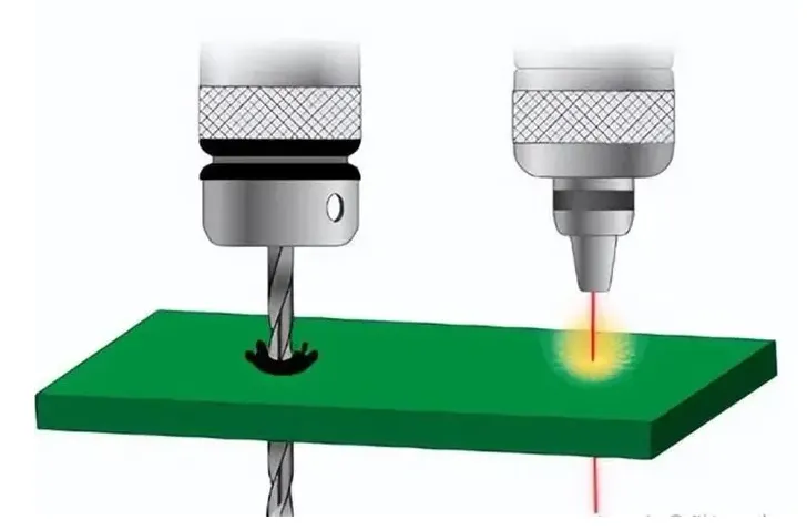
2. Laser Drilling for Microvias
Laser drilling is a cornerstone of HDI technology, enabling the creation of microvias for high-density designs. This technique supports larger board sizes by allowing more efficient use of space, as microvias take up less area than traditional vias. For example, a 20-layer HDI board might include thousands of microvias, supporting a size of 16 x 12 inches without routing issues.
3. Advanced Materials
Using high-performance materials like low-loss dielectrics can improve signal integrity and thermal management, allowing for larger multilayer PCBs. Materials with a dielectric constant (Dk) of 3.0 or lower are ideal for high-frequency applications, as they reduce signal loss over long traces, supporting bigger board dimensions.
Practical Tips for Engineers: Designing Larger PCBs with High Layer Counts
For engineers looking to design larger PCBs with high layer counts, consider the following actionable tips:
- Collaborate Early with Fabricators: Discuss size and layer count limitations with your manufacturing partner to identify feasible dimensions and avoid costly redesigns.
- Prioritize HDI for Density: Use HDI technology to pack more functionality into a smaller footprint, potentially allowing for larger overall sizes without sacrificing performance.
- Simulate Signal Integrity: Use simulation tools to model signal behavior on larger boards, ensuring that high layer counts don’t degrade performance.
- Balance Cost and Complexity: While more layers enable complex designs, they also increase costs. Optimize layer count to meet performance needs without exceeding budget constraints for larger boards.
Conclusion: Navigating Layer Count and PCB Size for Optimal Design
The interplay between PCB layer count and size is a critical consideration for engineers designing modern electronics. While higher layer counts enable greater functionality and complexity, they often impose limits on maximum achievable size due to manufacturing, thermal, and signal integrity challenges. By leveraging multilayer PCB design best practices, adopting HDI PCB technology, and utilizing advanced PCB fabrication techniques, designers can push these boundaries to create larger, high-performance boards.


