 ALLPCB


In the fast-evolving world of smart devices, designing printed circuit boards (PCBs) for Internet of Things (IoT) applications is a complex task. Engineers must balance low power consumption, compact layouts, and robust wireless connectivity to meet the demands of modern wearables, sensors, and connected gadgets. This blog post dives deep into the core challenges of IoT PCB design and offers practical solutions to achieve optimal performance. Whether you're working on low power PCB design for IoT, compact PCB layouts for wearables, or integrating wireless connectivity with PCB antennas, this guide will help you navigate the process with actionable insights.
Why IoT PCB Design Matters for Smart Devices
IoT devices are everywhere—from fitness trackers and smart thermostats to industrial sensors and medical implants. These devices rely on carefully designed PCBs to function efficiently in small spaces, operate on minimal power, and maintain seamless connectivity. A well-designed PCB ensures that a smart device can run for extended periods on a single battery charge, fit into tiny enclosures, and communicate reliably over wireless networks. However, achieving this balance is no easy feat, as it involves tackling multiple challenges simultaneously.
In this comprehensive guide, we'll explore the key aspects of IoT PCB design, including power management, size constraints, and connectivity solutions. By understanding these elements, engineers can create boards that meet the unique needs of IoT applications.
Key Challenges in IoT PCB Design
Designing PCBs for IoT devices comes with a unique set of hurdles. Below, we break down the primary challenges engineers face when working on these projects, focusing on power, size, and connectivity.
1. Power Efficiency: Low Power PCB Design for IoT
One of the biggest challenges in IoT PCB design is minimizing power consumption. Many IoT devices, especially wearables and remote sensors, operate on small batteries with capacities as low as 100-300 mAh. Extending battery life is critical to ensure user satisfaction and reduce maintenance costs.
The primary goal of low power PCB design for IoT is to reduce energy usage during both active and idle states. This often involves selecting components with low quiescent current (often in the range of microamperes, e.g., 1-5 μA), implementing sleep modes, and optimizing power delivery networks. For instance, using a low-dropout (LDO) regulator with an efficiency of over 90% can significantly cut power losses compared to traditional linear regulators.
Additionally, engineers must consider dynamic power management techniques. Microcontrollers with multiple power modes, such as deep sleep (consuming less than 1 μA) and active mode (consuming 1-10 mA), allow devices to conserve energy when not in use. Proper placement of decoupling capacitors, typically in the range of 0.1 μF to 1 μF near power pins, also helps stabilize voltage and reduce noise, further enhancing efficiency.
2. Size Constraints: Compact PCB Layout for Wearables
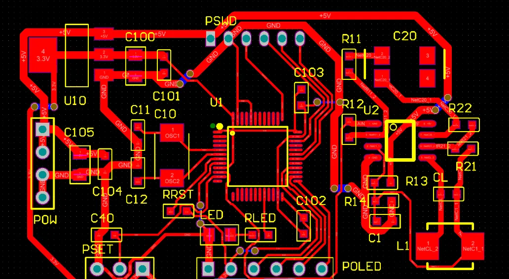
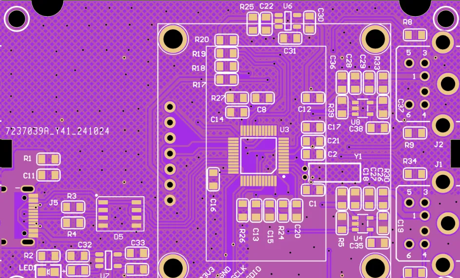
IoT devices, especially wearables like smartwatches and fitness bands, demand compact PCB layouts. Engineers often need to fit complex circuitry into spaces smaller than 20 mm x 20 mm while maintaining functionality. This requires a high-density interconnect (HDI) design approach, where components are packed tightly, and traces are routed with precision.
Compact PCB layouts for wearables often involve multi-layer boards, sometimes with 6-8 layers, to accommodate more components in less space. Surface-mount devices (SMDs) with package sizes as small as 0402 (0.4 mm x 0.2 mm) are commonly used to save space. However, such dense layouts increase the risk of signal interference and thermal issues, requiring careful planning of ground planes and heat dissipation paths.
Another strategy is to use flexible or rigid-flex PCBs, which can bend or fold to fit irregular shapes in wearable devices. These boards, often made from polyimide materials, allow for innovative designs but require precise stack-up planning to avoid mechanical stress on traces.
3. Connectivity: Wireless Connectivity PCB Antenna Design
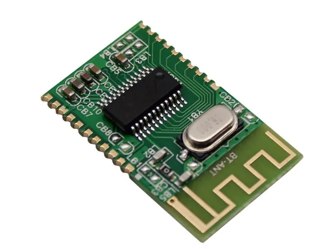
Wireless connectivity is the backbone of IoT devices, enabling communication via Wi-Fi, Bluetooth, Zigbee, or cellular networks like 4G and 5G. Integrating a reliable PCB antenna or supporting external antenna connections is a critical aspect of IoT PCB design. However, achieving strong wireless performance in a small form factor poses significant challenges.
PCB antennas, such as trace antennas or chip antennas, are popular for compact designs due to their low cost and small size. For example, a Bluetooth PCB trace antenna might operate at 2.4 GHz with a wavelength of approximately 12.5 cm, requiring a quarter-wave length of about 3.1 cm for optimal performance. However, fitting this into a small board often means compromising on efficiency or using meandered traces to reduce the physical size.
Signal integrity is another concern. Engineers must ensure minimal interference by maintaining proper impedance matching, typically targeting 50 ohms for most RF circuits. A poorly matched antenna can result in signal losses of up to 50% or more, drastically reducing the device's communication range. Using RF simulation tools to analyze return loss (S11 parameter) and placing ground planes strategically can help mitigate these issues.
Solutions for Effective IoT PCB Design
Now that we've covered the main challenges, let's explore practical solutions to address these issues and create high-performing IoT PCBs. These strategies focus on balancing power, size, and connectivity for smart devices.
1. Optimizing Power Management
To achieve low power PCB design for IoT, start by selecting energy-efficient components. Look for microcontrollers with built-in power-saving modes and low quiescent current. For instance, some modern MCUs consume as little as 0.5 μA in deep sleep mode, making them ideal for battery-powered devices.
Next, design the power delivery network (PDN) to minimize losses. Use switching regulators with efficiencies above 85% instead of linear regulators for higher current loads. Place bypass capacitors close to power pins to reduce voltage ripples, ensuring stable operation even under varying loads.
Software optimization also plays a role. Implement firmware that activates peripherals only when needed, reducing active power draw. For example, a sensor reading temperature data might wake up every 10 seconds for a brief 1-ms measurement, consuming minimal energy.
2. Mastering Compact Layouts
For compact PCB layouts in wearables, prioritize component placement and routing. Place critical components like processors and RF modules first, ensuring short trace lengths to minimize signal delays and interference. Use via-in-pad technology on multi-layer boards to save space, though this requires careful manufacturing considerations to avoid solder issues.
Thermal management is vital in dense designs. Use thermal vias to transfer heat from high-power components to a ground plane or heat sink. Ensure that the board's copper thickness, often 1 oz/ft2 or 2 oz/ft2, supports heat dissipation without adding unnecessary bulk.
Finally, leverage design software with auto-routing and design rule checks (DRC) to optimize layouts. These tools help identify spacing violations or potential crosstalk issues before fabrication, saving time and reducing errors in compact designs.
3. Enhancing Wireless Connectivity
For robust wireless connectivity with PCB antennas, start by choosing the right antenna type for your design. Chip antennas are ideal for ultra-small devices, while trace antennas work well when board space allows for custom patterns. Ensure the antenna is placed away from noisy components like switching regulators, which can introduce electromagnetic interference (EMI).
Impedance matching is critical for maximizing signal strength. Use a network of inductors and capacitors (pi-network) to tune the antenna to 50 ohms, and verify performance with a vector network analyzer (VNA) to measure return loss. A return loss of -10 dB or better indicates good matching, ensuring efficient power transfer.
Also, consider the device's enclosure during design. Plastic enclosures typically have less impact on RF signals, while metal ones can detune the antenna, reducing range by up to 30%. If a metal enclosure is unavoidable, allocate space for an external antenna connection to maintain performance.
Emerging Trends in IoT PCB Design
As IoT technology advances, new trends are shaping PCB design practices. Staying ahead of these developments can give engineers a competitive edge in creating next-generation smart devices.
One trend is the adoption of 5G connectivity for IoT. With data rates up to 10 Gbps and latency as low as 1 ms, 5G enables real-time applications like autonomous vehicles and remote surgery. However, designing PCBs for 5G requires handling higher frequencies (up to 28 GHz or more), necessitating advanced materials like low-loss laminates with dielectric constants below 3.0 to minimize signal loss.
Another trend is the integration of AI and machine learning directly on IoT devices. Edge computing reduces latency by processing data locally, but it demands more powerful processors on compact boards. This pushes designers to balance power and performance, often using system-on-chip (SoC) solutions that combine CPU, memory, and connectivity in a single package.
Lastly, sustainability is becoming a focus. Engineers are exploring eco-friendly materials and designing for recyclability, ensuring IoT devices have a smaller environmental footprint. This includes using lead-free solder and minimizing material waste during PCB fabrication.

Conclusion: Achieving Balance in IoT PCB Design
Designing PCBs for IoT applications is a delicate balancing act between power efficiency, compact size, and reliable connectivity. By addressing IoT PCB design challenges with targeted strategies—like optimizing power management for low power PCB design in IoT, mastering compact PCB layouts for wearables, and enhancing wireless connectivity with PCB antennas—engineers can create smart devices that meet modern demands.
At ALLPCB, we understand the complexities of IoT PCB design and are committed to supporting engineers with high-quality manufacturing and assembly services. Whether you're prototyping a new wearable or scaling production for industrial sensors, our expertise ensures your designs come to life with precision and reliability. Embrace these best practices, stay updated on emerging trends, and build the future of connected technology with confidence.


