 ALLPCB


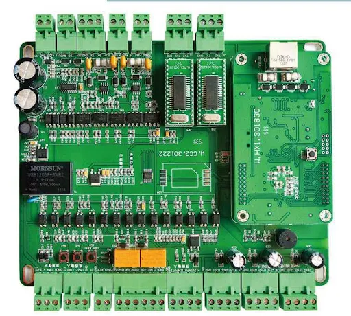
In the fast-evolving world of Internet of Things (IoT) devices, creating reliable and efficient printed circuit boards (PCBs) is crucial. IoT PCB assembly requires precision, attention to detail, and the right techniques to ensure devices perform seamlessly in connected environments. Whether you're working on smart home gadgets, industrial sensors, or wearable tech, following best practices in PCB assembly can make all the difference. In this comprehensive guide, we'll explore key methods like surface mount technology PCB assembly, through hole PCB assembly, reflow soldering PCB, wave soldering PCB, and automated optical inspection PCB to help you achieve top-tier results.
At ALLPCB, we understand the unique challenges of IoT manufacturing. This blog will dive into actionable tips and strategies to optimize your PCB assembly process, ensuring durability, efficiency, and cost-effectiveness for your IoT projects. Let's get started with the essentials of reliable manufacturing.
Why IoT PCB Assembly Demands Precision
IoT devices are often small, complex, and packed with functionality. They must operate reliably in diverse conditions—think of a smart thermostat exposed to temperature swings or an industrial sensor enduring vibrations. Poor PCB assembly can lead to failures like signal interference, power loss, or complete device breakdown. For instance, a misaligned component in a surface mount technology PCB assembly could disrupt a critical connection, causing data loss in an IoT network.
Moreover, IoT devices frequently handle high-speed signals, often in the range of 1-5 GHz for wireless communication. If impedance isn't controlled—typically targeting 50 ohms for RF lines—signal integrity suffers. By prioritizing best practices in assembly, you can minimize these risks and ensure your IoT products meet performance expectations.
Key Techniques in IoT PCB Assembly
IoT PCB assembly involves multiple techniques, each suited to different components and design needs. Below, we break down the most common methods and how to apply them effectively.
1. Surface Mount Technology PCB Assembly (SMT)
Surface mount technology PCB assembly is the go-to method for most IoT devices due to its ability to support compact designs. In SMT, components are mounted directly onto the surface of the PCB, allowing for smaller footprints and higher component density. This is ideal for IoT applications where space is limited, such as in smartwatches or wireless modules.
Best Practices for SMT in IoT:
- Precise Placement: Use automated pick-and-place machines to ensure components are positioned accurately. Misplacement by even 0.1 mm can lead to connection issues.
- Solder Paste Quality: Apply high-quality solder paste with consistent viscosity to avoid defects like tombstoning, where components lift during soldering.
- Thermal Management: IoT devices often generate heat in tight spaces. Design PCBs with thermal vias and ensure components rated for high temperatures (up to 125°C) are used.
By optimizing surface mount technology PCB assembly, you can achieve faster production cycles and reliable performance for miniature IoT systems.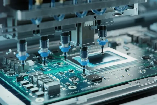
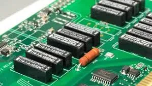
2. Through Hole PCB Assembly (THT)
While SMT dominates modern designs, through hole PCB assembly remains relevant for IoT applications requiring robust mechanical strength. In THT, component leads are inserted through holes in the PCB and soldered on the opposite side. This method is often used for connectors, power components, or sensors in industrial IoT devices that face physical stress.
Best Practices for THT in IoT:
- Hole Sizing: Ensure hole diameters match component leads precisely, typically within a tolerance of ±0.05 mm, to avoid loose fits or soldering challenges.
- Component Selection: Choose components with leads that can withstand bending stress, especially for IoT devices exposed to vibration.
- Manual or Automated Assembly: For low-volume IoT prototypes, manual insertion may suffice, but for scalability, invest in automated THT assembly equipment.
Through hole PCB assembly provides durability for specific IoT use cases, ensuring long-term reliability in harsh environments.
Soldering Techniques for IoT PCB Assembly
Soldering is the backbone of PCB assembly, creating the electrical and mechanical bonds that hold components in place. For IoT manufacturing, two primary soldering methods stand out: reflow soldering and wave soldering.
3. Reflow Soldering PCB
Reflow soldering PCB is the preferred technique for SMT components in IoT assembly. In this process, solder paste is applied to the PCB, components are placed, and the board is heated in a reflow oven. The solder melts and solidifies, forming strong connections. This method is ideal for high-density IoT boards with tiny components like 0402 resistors or QFN packages.
Best Practices for Reflow Soldering in IoT:
- Temperature Profile: Follow a precise thermal profile, typically peaking at 245-260°C for lead-free solder, to prevent thermal shock to sensitive IoT components.
- Stencil Design: Use laser-cut stencils with apertures sized at 1:1 or slightly reduced (90%) to control solder paste volume and avoid bridging.
- Environment Control: Maintain a clean, dust-free environment to prevent contamination of solder paste, which can cause defects.
Reflow soldering PCB ensures consistent, high-quality joints, critical for the compact and complex nature of IoT designs.
4. Wave Soldering PCB
Wave soldering PCB is commonly used for through-hole components or mixed-technology boards in IoT assembly. During this process, the PCB passes over a wave of molten solder, which coats the exposed leads and creates connections. It's a fast, cost-effective method for larger components or boards with fewer SMT parts.
Best Practices for Wave Soldering in IoT:
- Flux Application: Apply flux evenly to clean leads and pads, ensuring proper solder flow and minimizing defects like cold joints.
- Solder Temperature: Keep solder bath temperature around 260-270°C for lead-free alloys to ensure proper wetting without damaging the PCB.
- Masking SMT Areas: Protect SMT components on mixed boards with heat-resistant tape or masks to avoid damage during the wave process.
Wave soldering PCB offers efficiency for specific IoT assemblies, balancing speed and reliability for through-hole-heavy designs.
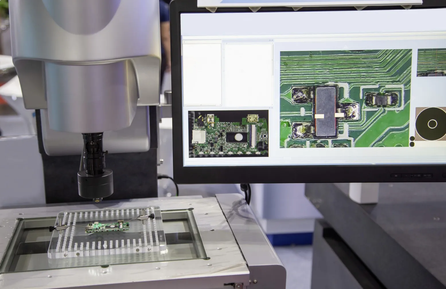
Ensuring Quality with Automated Optical Inspection PCB
Quality control is non-negotiable in IoT PCB assembly. Even a single defect can render a device unusable, leading to costly recalls or customer dissatisfaction. Automated optical inspection PCB (AOI) is a powerful tool to catch issues early. AOI systems use high-resolution cameras and software to scan assembled PCBs for defects like misaligned components, solder bridges, or missing parts.
Best Practices for AOI in IoT:
- Post-Reflow Inspection: Perform AOI immediately after reflow soldering to detect issues like tombstoning or insufficient solder before further processing.
- High-Resolution Settings: Configure AOI systems to detect defects as small as 0.01 mm, critical for tiny IoT components like 0201 packages.
- Data Feedback: Use AOI data to refine upstream processes, such as adjusting pick-and-place accuracy or solder paste application.
Automated optical inspection PCB ensures that every IoT board meets strict quality standards, reducing the risk of field failures and enhancing customer trust.
Additional Tips for Reliable IoT PCB Manufacturing
Beyond the core assembly techniques, several overarching strategies can elevate your IoT PCB manufacturing process. These tips focus on design, material selection, and scalability to ensure long-term success.
Design for Manufacturability (DFM): Start with a DFM approach to simplify assembly. For example, minimize the number of unique components to reduce inventory complexity, and ensure pad sizes comply with industry standards like IPC-7351 for reliable soldering.
Material Selection: Choose PCB substrates like FR-4 with a high glass transition temperature (Tg of 170°C or more) for IoT devices exposed to heat. For RF-heavy IoT applications, consider low-loss materials like Rogers laminates to maintain signal integrity at frequencies above 2 GHz.
Testing and Prototyping: Before full-scale production, conduct thorough testing on prototypes. Use in-circuit testing (ICT) to verify electrical connections and functional testing to simulate real-world IoT use cases, ensuring reliability under load.
Scalability: Partner with a manufacturing service that can scale with your needs. Look for capabilities in both low-volume prototyping and high-volume production to avoid delays as your IoT product grows in demand.
Overcoming Common Challenges in IoT PCB Assembly
IoT PCB assembly comes with unique hurdles, from miniaturization to power efficiency. Here are some common issues and how to address them:
- Miniaturization: As IoT devices shrink, component spacing tightens. Use micro-vias (diameters as small as 0.1 mm) and HDI (high-density interconnect) designs to fit more functionality into less space.
- Power Constraints: Many IoT devices run on batteries. Optimize power delivery networks (PDNs) with low-impedance paths (targeting under 0.5 ohms) to minimize voltage drops.
- Signal Interference: With multiple wireless protocols like Wi-Fi and Bluetooth on a single IoT board, interference is a risk. Implement proper grounding and shielding, maintaining at least 0.2 mm separation between high-speed traces.
By anticipating these challenges, you can build IoT PCBs that perform reliably in real-world conditions.
Conclusion: Building Better IoT Devices with ALLPCB
IoT PCB assembly is a complex but rewarding process when done right. By mastering techniques like surface mount technology PCB assembly, through hole PCB assembly, reflow soldering PCB, wave soldering PCB, and automated optical inspection PCB, you can create IoT devices that are both reliable and efficient. At ALLPCB, we're committed to supporting your journey with cutting-edge manufacturing solutions tailored to IoT needs.
Whether you're designing a new smart sensor or scaling up production for a connected product, these best practices will guide you toward success. Focus on precision, quality, and scalability to ensure your IoT devices stand out in a competitive market. With the right approach, your PCBs will power the next generation of connected innovation.


