ALLPCB


Reducing the size of a printed circuit board (PCB) is a critical goal for many engineers, especially when designing compact devices for industries like wearables, IoT, and mobile technology. The key to achieving a smaller PCB lies in effective component placement, along with strategies like optimal component orientation, reducing vias, single-layer PCB design, and maximizing space. In this guide, we'll explore actionable techniques to shrink your PCB footprint while maintaining performance and reliability. Let's dive into the details of how to make your designs more compact and efficient.
Why Reducing PCB Size Matters
In today’s fast-paced tech world, smaller devices are often synonymous with better design. A compact PCB allows for sleeker products, reduces material costs, and can improve signal integrity by shortening trace lengths. However, shrinking a PCB without sacrificing functionality requires careful planning, especially in component placement. Poor placement can lead to issues like signal interference, overheating, or manufacturing challenges. By focusing on smart layout strategies, you can achieve a smaller board that still performs at its best.
Key Strategies for Reducing PCB Size with Component Placement
Component placement is the foundation of a compact PCB design. The way you position parts on the board directly impacts the space you use, the length of traces, and the overall efficiency of the layout. Below are proven strategies to help you minimize PCB size through effective placement.
1. Prioritize Optimal Component Orientation
One of the simplest yet most impactful ways to save space is by focusing on optimal component orientation. Rotating components to align their pins or connectors in a way that shortens trace lengths can significantly reduce the board area needed. For instance, placing a microcontroller so its input/output pins face nearby components can cut down on routing space by up to 20% in some designs.
Additionally, consider the physical shape of components. Surface-mount devices (SMDs) like resistors or capacitors can often be rotated 90 degrees to fit into tighter spaces without affecting performance. Pay attention to datasheets for orientation restrictions, especially for polarized components like diodes or electrolytic capacitors, to avoid functionality issues.
Tip: Use design software with auto-placement features to experiment with different orientations. Look for layouts where traces are shortest and components are packed closely without violating clearance rules (typically 0.2 mm to 0.3 mm between components for standard designs).
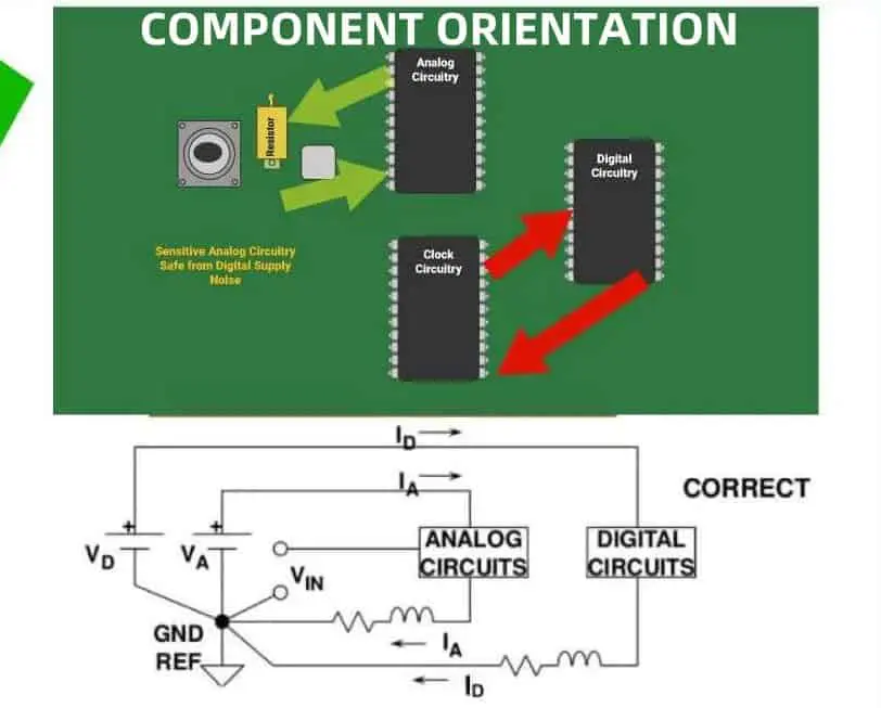
2. Group Related Components Together
Grouping components that work together functionally can drastically reduce the board space needed for traces. For example, place decoupling capacitors as close as possible to the power pins of an IC—ideally within 1 mm to 2 mm—to minimize noise and save routing space. Similarly, keep analog and digital components in separate zones to avoid interference while reducing the need for long, winding traces across the board.
This approach not only saves space but also improves signal integrity. Shorter traces mean less resistance and lower chances of electromagnetic interference (EMI). A well-grouped layout can reduce trace lengths by 15-30%, directly contributing to a smaller PCB footprint.
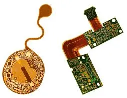
3. Leverage Both Sides of the PCB When Possible
While single-layer PCB designs are often preferred for cost and simplicity, using both sides of a double-sided board can significantly cut down on size. Place smaller, less critical components like resistors or LEDs on the bottom layer, reserving the top layer for larger ICs or connectors. This maximizes space usage and can reduce board dimensions by up to 40% compared to a single-layer layout with the same components.
However, be mindful of manufacturing constraints. Ensure that components on the bottom layer won’t interfere with soldering processes or assembly. Also, keep thermal management in mind—avoid placing heat-sensitive parts on the bottom where airflow might be limited.
Advanced Techniques for PCB Size Reduction
Beyond basic placement, there are advanced strategies that can further shrink your PCB while maintaining performance. These techniques require a deeper understanding of design rules and manufacturing processes but offer substantial space-saving benefits.
4. Focus on Reducing Vias for a Compact Design
Vias, which connect different layers of a PCB, take up valuable space and can complicate routing in a compact design. Reducing vias is a powerful way to save space, especially in single-layer or double-layer boards. Each via typically requires a pad diameter of 0.5 mm to 0.8 mm, plus clearance space, which adds up quickly in dense layouts.
To minimize vias, prioritize single-layer routing where possible. Route traces on the same layer to avoid unnecessary transitions between layers. If vias are unavoidable, use micro vias (diameters below 0.15 mm) if your manufacturer supports them, as they occupy less space than standard through-hole vias. Additionally, plan your component placement to align pins that need to connect on the same layer, reducing the need for layer-switching.
5. Explore Single-Layer PCB Design for Ultra-Compact Boards
For very small or cost-sensitive projects, single-layer PCB design can be a game-changer. Single-layer boards use only one conductive layer, which forces you to optimize component placement and routing to fit everything in a limited space. While this approach isn’t suitable for complex circuits with high component density, it’s ideal for simpler designs like basic sensor modules or LED drivers.
To succeed with a single-layer layout, place components in a grid-like pattern to simplify trace routing. Avoid crossing traces by carefully planning the sequence of connections, and use jumpers (short wires) if absolutely necessary to bridge over traces. A well-executed single-layer design can reduce board size by 30-50% compared to multi-layer alternatives for basic circuits.
Caution: Single-layer designs can limit performance in high-speed or noise-sensitive applications due to longer traces and lack of ground planes. Always evaluate your project’s needs before committing to this approach.
6. Maximize Space with Creative Layout Techniques
Maximizing space on a PCB often means thinking outside the box. Nested layouts, where smaller components are tucked under larger ones (like placing resistors under a microcontroller package), can save significant space if clearance rules allow. Be sure to check for height restrictions and thermal dissipation needs before nesting components.
Another technique is to use irregular board shapes. Instead of sticking to a rectangular PCB, design the board to match the shape of your enclosure or device. This can eliminate unused areas and reduce the overall footprint by 10-20% in some cases. Finally, consider stacking components vertically using mezzanine connectors or 3D assembly if your design allows for it—this effectively doubles the usable area without increasing the board’s length or width.
Tools and Tips for Effective Component Placement
Modern design software plays a huge role in achieving a compact PCB layout. Most tools offer features like auto-placement and design rule checks (DRC) to help you optimize component positioning. Start by defining your board constraints—such as minimum clearance (e.g., 0.2 mm) and trace width (e.g., 0.1 mm for low-current signals)—to ensure the software suggests feasible layouts.
Manually adjust placements after auto-placement to fine-tune for space efficiency. Focus on high-priority components first, like power ICs or connectors, and build the layout around them. Regularly simulate signal integrity to ensure that your compact design doesn’t introduce issues like crosstalk or excessive impedance (aim for impedance values around 50 ohms for high-speed signals).
Tip: Always leave a small buffer space—around 5-10% of the board area—for future modifications or unexpected design changes. This prevents the need for a complete redesign if components or requirements shift.
Common Mistakes to Avoid When Reducing PCB Size
While striving for a smaller PCB, it’s easy to make mistakes that compromise performance or manufacturability. Avoid these common pitfalls:
- Overcrowding Components: Packing parts too closely can lead to soldering issues or thermal problems. Maintain at least 0.3 mm clearance between components unless specified otherwise by your manufacturer.
- Ignoring Thermal Management: Compact designs often struggle with heat dissipation. Place heat-generating components near edges or use thermal vias (0.3 mm diameter) to transfer heat to other layers.
- Neglecting Signal Integrity: Shortening traces is great, but don’t compromise critical signal paths. High-speed signals may require controlled impedance (e.g., 50 ohms) or specific routing lengths.
Conclusion: Build Smaller, Smarter PCBs
Reducing PCB size through effective component placement is both an art and a science. By focusing on optimal component orientation, reducing vias, exploring single-layer PCB design, and maximizing space, you can create compact boards that meet the demands of modern electronics without sacrificing performance. Start with a clear plan, use design tools to experiment with layouts, and always prioritize functionality alongside size reduction.
Implementing these strategies can help you achieve significant space savings—often reducing board area by 20-50% depending on the complexity of your design. With careful planning and attention to detail, your next PCB project can be smaller, more efficient, and ready for the challenges of cutting-edge technology.