 ALLPCB


In the world of high-power electronics, designing a PCB that can handle significant current without overheating or failing is a critical challenge. Heavy copper PCBs are the go-to solution for such applications, offering enhanced current capacity and thermal management. But how can you maximize current capacity while keeping trace widths as minimal as possible? The key lies in optimizing copper thickness, material selection, and design techniques tailored for high-current demands. In this comprehensive guide, we'll dive deep into heavy copper PCB design, exploring strategies to achieve high current capacity with efficient layouts for applications like power electronics, automotive systems, and industrial equipment.
What Are Heavy Copper PCBs and Why Do They Matter?
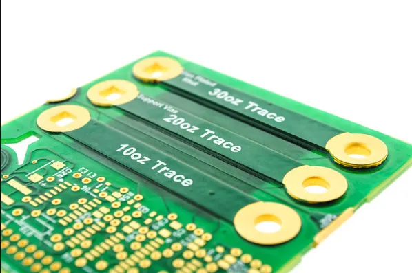
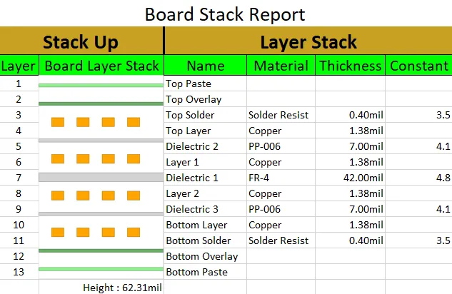
Heavy copper PCBs are printed circuit boards with thicker copper layers compared to standard PCBs. While a typical PCB might have copper layers of 1 oz/ft2 (about 35 micrometers thick), heavy copper PCBs start at 3 oz/ft2 (105 micrometers) and can go up to 20 oz/ft2 or more in extreme cases. This increased copper thickness allows the board to carry higher currents, dissipate heat more effectively, and withstand harsh operating conditions.
For industries dealing with high power PCB applications—think electric vehicle chargers, renewable energy inverters, and industrial motor controls—heavy copper is essential. It reduces the risk of thermal stress and trace burnout, ensuring reliability in demanding environments. But thicker copper alone isn’t enough; smart design choices are needed to balance current capacity with space constraints, which is where minimizing trace width comes into play.
Understanding Copper Thickness and Current Capacity
The relationship between copper thickness and current capacity is fundamental to high current PCB design. The thicker the copper layer, the more current a trace can carry without overheating. According to the IPC-2221 standard, a 1 oz/ft2 copper trace with a width of 100 mils (2.54 mm) can handle approximately 4.5 amps at a 10°C temperature rise. In contrast, a 3 oz/ft2 copper trace of the same width can handle around 9 amps under similar conditions. This demonstrates how increasing copper thickness directly boosts current capacity.
However, wider traces also take up more board space, which can be a limiting factor in compact designs. The goal is to use heavier copper to increase current capacity while keeping trace widths as narrow as possible. For instance, a 6 oz/ft2 copper trace at 50 mils wide can carry roughly 8 amps with a 10°C temperature rise, compared to a 1 oz/ft2 trace needing over 200 mils width for the same current. This space-saving potential is why heavy copper is a game-changer for high-power designs.
To calculate the required trace width for a specific current, you can use online calculators based on IPC standards or refer to current capacity charts. These tools factor in copper thickness, ambient temperature, and allowable temperature rise to provide precise measurements for your design.
Key Design Strategies for Maximizing Current Capacity
Designing a heavy copper PCB for high current applications involves more than just increasing copper thickness. Below are proven strategies to optimize current capacity while minimizing trace width.
1. Select the Right Copper Thickness for Your Needs
Choosing the appropriate copper weight is the first step. For moderate high-current applications, 3-4 oz/ft2 might suffice, while extreme power designs may require 6-10 oz/ft2 or more. Keep in mind that thicker copper increases manufacturing costs and can complicate etching processes, so balance performance with budget constraints. Assess your current requirements using simulation tools to avoid over-specifying copper weight, which can unnecessarily drive up costs.
2. Optimize Trace Layout for Efficiency
Efficient trace routing is critical in high power PCB designs. Keep high-current traces as short and direct as possible to minimize resistance and heat buildup. Avoid sharp corners in trace paths, as they can create current concentration points that lead to hotspots. Instead, use 45-degree angles or curved traces to ensure smooth current flow. Additionally, distribute current evenly across parallel traces if a single trace cannot handle the load, effectively reducing the width needed per trace.
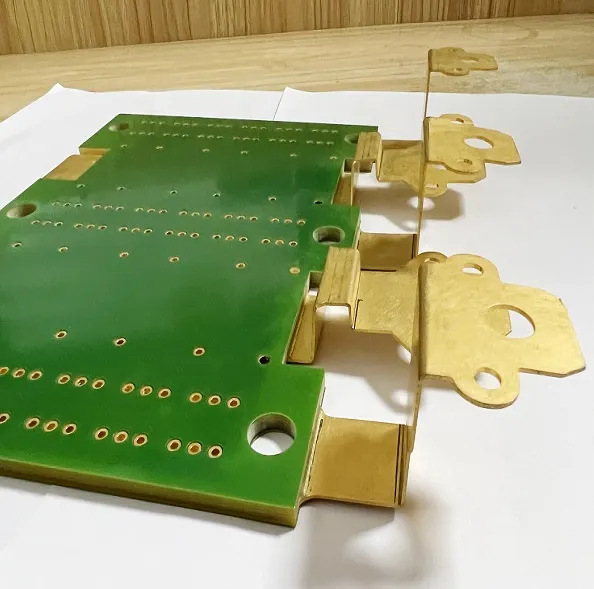
3. Incorporate PCB Busbars for Ultra-High Currents
For applications requiring currents beyond what even heavy copper traces can handle, PCB busbars are an excellent solution. A busbar is a thick copper strip or bar integrated into or mounted on the PCB to carry massive currents—sometimes hundreds of amps. By offloading the heaviest current loads to busbars, you can keep trace widths on the board minimal while still meeting power demands. Busbars also improve thermal dissipation, reducing the risk of overheating in high-current zones.
4. Use Multiple Copper Layers to Distribute Current
In multilayer PCBs, stacking copper layers can significantly boost current capacity without increasing trace width. For example, if a single 3 oz/ft2 layer can carry 9 amps on a 100-mil trace, using two such layers in parallel effectively doubles the capacity to 18 amps for the same trace width. This technique is particularly useful in space-constrained designs where widening traces isn’t an option. Ensure proper via placement to connect layers and distribute current evenly, avoiding bottlenecks.
5. Enhance Thermal Management
Heat is the enemy of high-current designs. Excess heat can degrade components and reduce the lifespan of your PCB. Heavy copper naturally aids in heat dissipation due to its higher thermal conductivity, but additional measures can further improve performance. Add thermal vias near high-current traces to transfer heat to other layers or a heatsink. Consider using exposed copper pads or planes to act as heat spreaders, especially in areas with high power dissipation.
High Current PCB Materials: Beyond Copper Thickness
While copper thickness is the star of the show, the choice of substrate material and other design elements also impacts current capacity and thermal performance. Let’s explore the role of materials in heavy copper PCB design.
Substrate Materials for High Power Applications
Standard FR-4 substrates are common in many PCBs, but they may not withstand the thermal stress of high-current applications. For heavy copper designs, consider advanced materials like high-Tg FR-4 (with a glass transition temperature above 170°C), polyimide, or ceramic-based substrates. These materials offer better thermal stability and can handle the elevated temperatures associated with high power PCB operation. For example, polyimide substrates can operate at temperatures up to 250°C, making them ideal for automotive and aerospace applications.
Surface Finishes for Durability
The surface finish on a heavy copper PCB affects both solderability and long-term reliability under high current. Electroless Nickel Immersion Gold (ENIG) is a popular choice for its corrosion resistance and smooth surface, though it may not be ideal for extremely high currents due to potential nickel diffusion. Hot Air Solder Leveling (HASL) with lead-free solder is a cost-effective alternative that works well for heavy copper, providing a robust coating that withstands thermal cycling.
Challenges in Heavy Copper PCB Design
While heavy copper offers many benefits, it also comes with unique challenges that designers must address to ensure success.
Manufacturing Limitations
Thicker copper layers are harder to etch precisely, which can lead to inconsistencies in trace width and spacing. This is especially problematic for very fine traces or dense layouts. Work closely with your PCB manufacturer to understand their capabilities and design within those constraints. For instance, minimum trace widths and spacing may need to be larger for 6 oz/ft2 copper compared to 1 oz/ft2.
Cost Considerations
Heavier copper and advanced materials increase the cost of PCB fabrication. Additionally, designs with extreme copper weights (above 10 oz/ft2) often require specialized processes, further driving up expenses. Optimize your design by using heavy copper only where necessary—such as high-current paths—and standard copper elsewhere to keep costs manageable.
Mechanical Stress
Thicker copper can introduce mechanical stress during thermal expansion, potentially causing delamination or cracking in the substrate. To mitigate this, ensure proper adhesion between layers and consider using materials with matched coefficients of thermal expansion (CTE). Reinforcing the board with additional vias or anchors can also help maintain structural integrity.
Applications of Heavy Copper PCBs in High Power Designs
Heavy copper PCBs shine in industries where high current and reliability are non-negotiable. In automotive systems, they power electric vehicle battery management systems and charging stations, handling currents of 50 amps or more. In renewable energy, heavy copper is used in solar inverters and wind turbine controllers to manage high power loads efficiently. Industrial applications like motor drives and welding equipment also rely on these boards to deliver consistent performance under extreme conditions.
Conclusion: Balancing Current Capacity and Design Efficiency
Heavy copper PCBs are a powerful solution for high-current applications, offering the ability to carry substantial loads while maintaining reliability. By carefully selecting copper thickness, optimizing trace layouts, incorporating PCB busbars, and leveraging multilayer designs, you can maximize current capacity without sacrificing valuable board space. Pair these techniques with the right materials and thermal management strategies to ensure your high power PCB performs flawlessly even in the toughest environments.
Designing for high current doesn’t have to mean bulky traces or oversized boards. With the insights and strategies shared in this guide, you can achieve efficient, compact designs that meet the demands of modern power electronics. Whether you’re working on automotive, industrial, or energy projects, heavy copper PCB design opens the door to innovation and performance.


