 ALLPCB


Designing heavy copper PCBs is a powerful way to handle high-power applications, but thermal management is a critical challenge that must be addressed. How do you overcome heat buildup in heavy copper PCBs? The answer lies in strategic design techniques like using thermal vias, optimizing copper thickness, and incorporating effective cooling methods. In this blog post, we'll dive deep into the world of heavy copper PCB thermal management, exploring practical solutions for heat dissipation and cooling to ensure reliability and performance in demanding applications.
What Are Heavy Copper PCBs and Why Thermal Management Matters
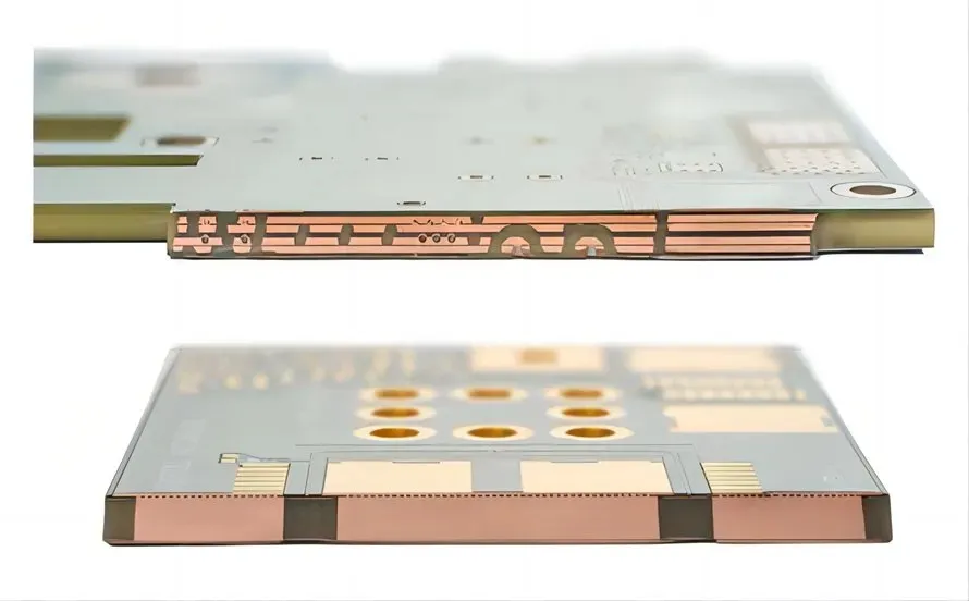
Heavy copper PCBs are printed circuit boards with copper thicknesses significantly higher than standard boards, typically ranging from 3 oz/ft2 to 20 oz/ft2 or more. These boards are used in high-power applications such as power supplies, automotive electronics, and industrial equipment, where they handle large currents and voltages. While the thicker copper enhances current-carrying capacity and durability, it also generates substantial heat due to resistive losses.
Without proper heavy copper PCB thermal management, excessive heat can lead to component failure, reduced lifespan, and compromised performance. Effective heat dissipation is essential to maintain the integrity of the board and ensure safe operation under high-power conditions. Let's explore the core challenges and solutions for managing heat in these specialized boards.
Key Thermal Challenges in Heavy Copper PCB Design
Heavy copper PCBs face unique thermal challenges due to their design and application. Understanding these issues is the first step toward implementing effective solutions for heavy copper PCB heat dissipation.
1. High Heat Generation from Increased Current
Thicker copper layers allow heavy copper PCBs to carry higher currents, often exceeding 50 amps in some applications. However, as current flows through the copper, resistive heating occurs, following the formula P = I2R, where P is power (heat) dissipated, I is current, and R is resistance. Even with copper’s low resistance, the heat generated can be significant at high currents, leading to temperature rises of 30°C or more above ambient levels if not managed properly.
2. Limited Heat Dissipation in Confined Spaces
Many high-power applications require compact designs, leaving little room for heat to escape naturally. Without adequate heavy copper PCB cooling, hot spots can form, especially near power components like MOSFETs or inductors, where localized temperatures can exceed 100°C, risking thermal runaway or solder joint failure.
3. Thermal Expansion and Mechanical Stress
Heat causes materials in a PCB to expand at different rates, a phenomenon known as thermal expansion. Copper and the substrate material (often FR-4) have different coefficients of thermal expansion (CTE), with copper at approximately 17 ppm/°C and FR-4 at 14-18 ppm/°C. This mismatch can create mechanical stress, potentially leading to delamination or cracking over repeated thermal cycles.
Addressing these challenges requires a combination of design strategies focused on heavy copper PCB thermal management. Let’s look at the most effective techniques to dissipate heat and maintain optimal performance.
Effective Strategies for Heavy Copper PCB Thermal Management
Designing for heat dissipation in heavy copper PCBs involves multiple approaches, from material selection to layout optimization. Below are proven methods to tackle thermal challenges.
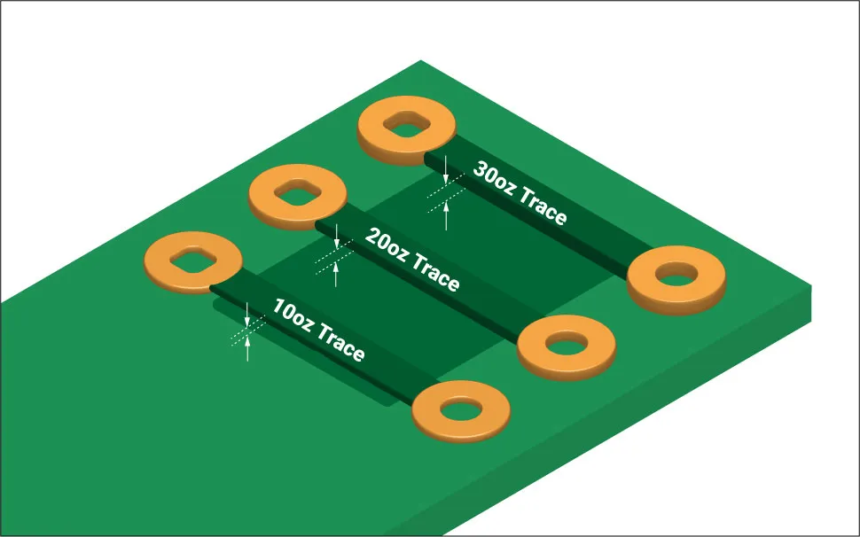
1. Optimizing Copper Thickness for Heat Distribution
While thicker copper can handle higher currents, it also concentrates heat if not distributed properly. A balanced approach is to use copper thicknesses tailored to the current requirements—often 6 oz/ft2 to 10 oz/ft2 for many high-power designs. Spreading copper across wider traces or planes helps distribute heat more evenly, reducing hot spots. For instance, a 10 oz/ft2 copper plane can lower thermal resistance by up to 20% compared to narrower traces of the same thickness.
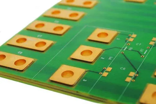
2. Incorporating Heavy Copper PCB Thermal Vias
Thermal vias are small, plated-through holes that transfer heat from one layer of the PCB to another, often connecting to a heat sink or a ground plane. In heavy copper PCB designs, thermal vias are critical for moving heat away from high-power components. A typical thermal via array might include 10-20 vias per square inch, each with a diameter of 0.3 mm to 0.5 mm, filled with conductive material to enhance thermal conductivity. Studies show that thermal vias can reduce component temperatures by 15-25°C in high-power setups.
When designing thermal vias, place them directly under or near heat-generating components. Ensure they connect to large copper planes on inner or bottom layers to maximize heat spreading. However, avoid overusing vias, as they can increase manufacturing costs and potentially weaken the board’s structure if not spaced properly.
3. Using High Thermal Conductivity Materials
The choice of substrate material plays a big role in heavy copper PCB heat dissipation. Standard FR-4 has a thermal conductivity of about 0.3 W/m·K, which is insufficient for high-power designs. Switching to materials like aluminum-backed substrates or ceramic-based materials with thermal conductivities of 1.5-3 W/m·K or higher can significantly improve heat transfer. For extreme cases, metal core PCBs (MCPCBs) with aluminum or copper cores offer thermal conductivities up to 200 W/m·K, making them ideal for heavy copper PCB cooling.
4. Adding Heat Sinks and External Cooling Solutions
For applications where passive heat dissipation isn’t enough, external cooling solutions become necessary. Heat sinks, made of aluminum or copper, can be attached to the PCB or directly to components to absorb and dissipate heat. A well-designed heat sink can reduce component temperatures by 20-40°C, depending on its surface area and airflow. In heavy copper PCB designs, ensure the heat sink is thermally connected to copper planes or thermal vias for maximum efficiency.
In more demanding environments, active cooling methods like fans or liquid cooling systems may be required. While these add complexity and cost, they can handle heat loads exceeding 100 W per component, making them suitable for industrial or automotive applications.
5. Strategic Component Placement and Layout Design
The physical layout of a heavy copper PCB can make or break its thermal performance. Place heat-generating components away from each other to prevent heat concentration. Position them near thermal vias or heat sinks for direct heat transfer. Additionally, avoid placing sensitive components, like microcontrollers, near hot zones where temperatures might exceed their operating limits (typically 85°C to 125°C).
Use copper pour areas as thermal planes to spread heat across the board. For multilayer designs, dedicate entire layers to ground or power planes with heavy copper to act as heat spreaders. This can lower the overall board temperature by 10-15°C compared to designs without thermal planes.
Advanced Techniques for Heavy Copper PCB Cooling
Beyond the basics, advanced techniques can further enhance thermal performance in heavy copper PCB designs, especially for cutting-edge applications.
1. Embedded Heat Pipes
Heat pipes are highly efficient heat transfer devices that use a liquid-vapor cycle to move heat away from hot spots. Embedding miniature heat pipes into a heavy copper PCB can target specific areas of high heat generation, reducing temperatures by up to 30% in some cases. While this approach increases design complexity and cost, it’s ideal for compact, high-power systems where space for traditional heat sinks is limited.
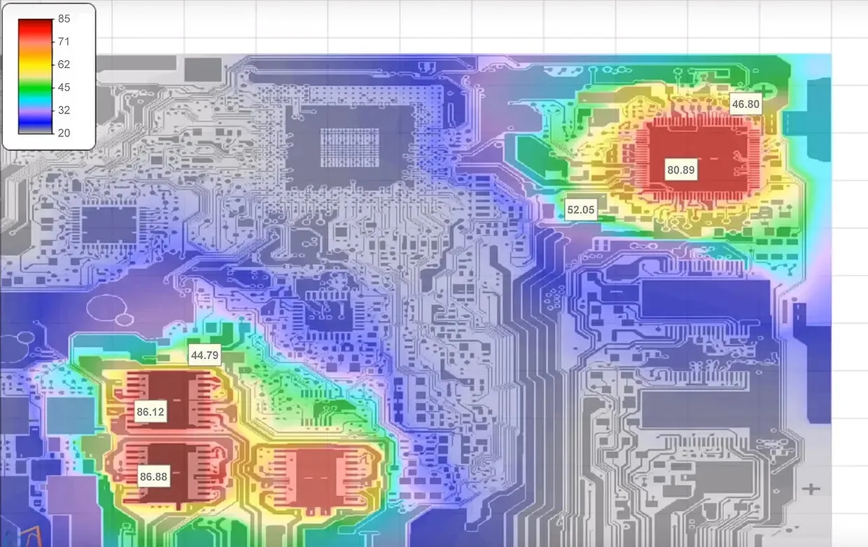
2. Thermal Simulation and Analysis
Before finalizing a design, use thermal simulation software to model heat distribution and identify potential hot spots. Tools can simulate temperature rises under various load conditions, allowing designers to optimize thermal vias, copper planes, and cooling solutions. For example, a simulation might reveal that a component reaches 110°C under a 50 W load, prompting the addition of more thermal vias or a larger heat sink to bring it below 85°C.
Practical Tips for Implementing Thermal Solutions
Here are some actionable tips to ensure success in managing heat in heavy copper PCB designs:
- Start with thermal budgeting early in the design phase. Estimate the heat generated by each component (using datasheets or formulas like P = I2R) and plan dissipation paths accordingly.
- Collaborate with your PCB manufacturer to confirm capabilities for heavy copper thicknesses and thermal via drilling. Not all manufacturers can handle copper beyond 10 oz/ft2 or complex via arrays.
- Test prototypes under real-world conditions to validate thermal performance. Use infrared cameras to detect hot spots and measure temperatures, ensuring they stay within safe limits (typically below 85°C for most components).
- Balance cost and performance. While advanced materials and cooling solutions improve heavy copper PCB thermal management, they can significantly increase production costs. Choose solutions that match your application’s needs.
Conclusion: Mastering Heavy Copper PCB Thermal Challenges
Heavy copper PCBs are indispensable for high-power applications, but their thermal challenges cannot be ignored. By focusing on heavy copper PCB heat dissipation through techniques like thermal vias, optimized copper distribution, high-conductivity materials, and external cooling solutions, designers can ensure reliability and performance. Advanced methods such as embedded heat pipes and thermal simulations further enhance heavy copper PCB cooling, especially in demanding environments.


