 ALLPCB


When designing high-current PCBs, one of the most critical factors to consider is the minimum line width for traces. So, what is the minimum line width for high-current applications? Simply put, it depends on the current load, copper thickness, and temperature rise limits, but as a general rule, traces carrying high currents often require widths of 0.5 mm or more for every 1-2 amps of current, based on standard copper thicknesses like 1 oz/ft2. This ensures safety, reliability, and effective thermal management. In this comprehensive guide, we’ll dive deep into the details of high current PCB trace width, minimum line width current capacity, and PCB thermal management trace width to help you design boards that perform optimally under demanding conditions.
Why Minimum Line Width Matters for High-Current PCBs
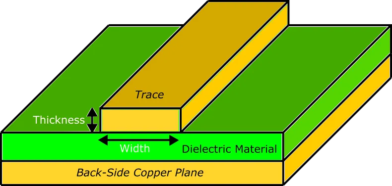
In PCB design, the width of a trace directly impacts its ability to carry current without overheating or failing. For high-current applications, such as power supplies, automotive electronics, or industrial systems, narrow traces can lead to excessive heat buildup, voltage drops, and even board failure. Determining the correct minimum line width current capacity is essential to prevent these issues and ensure long-term reliability.
Traces that are too thin for the current they carry will experience a rise in temperature due to resistance. If the temperature exceeds safe limits, it can damage components, degrade the board material, or cause delamination. By calculating the appropriate trace width, you can manage heat effectively and maintain the integrity of your design.
Understanding High Current PCB Trace Width: Key Factors
Designing for high-current applications requires a clear understanding of several factors that influence trace width. Let’s break these down to give you a solid foundation for your PCB layout.
1. Current Load and Trace Width Relationship
The amount of current a trace can safely carry is directly tied to its width and thickness. A wider trace has lower resistance, allowing it to handle more current without overheating. For example, with a copper thickness of 1 oz/ft2 (approximately 35 micrometers), a trace width of 0.5 mm can typically carry about 1.2 amps with a temperature rise of 10°C. If the current increases to 3 amps, the width may need to be around 1.5 mm or more under the same conditions.
To determine the exact width, you can use industry-standard calculators based on the IPC-2221 standard, which provides guidelines for trace width based on current, copper weight, and acceptable temperature rise. These tools help ensure that your design stays within safe limits for high current PCB trace width.
2. Copper Thickness and Its Impact
Copper thickness, often measured in ounces per square foot (oz/ft2), plays a big role in current-carrying capacity. Thicker copper layers can handle more current for the same trace width. For instance, a 2 oz/ft2 copper layer can carry roughly twice the current of a 1 oz/ft2 layer for the same width and temperature rise. High-current designs often use 2 oz/ft2 or even 3 oz/ft2 copper to reduce the required trace width and improve heat dissipation.
3. Temperature Rise and Thermal Management
Temperature rise is a critical consideration in PCB thermal management trace width. When current flows through a trace, it generates heat due to resistance. The acceptable temperature rise (often 10°C to 30°C above ambient) depends on the materials used and the operating environment. Wider traces reduce resistance and keep temperatures lower, which is vital for high-current applications where heat can accumulate quickly.
How to Calculate Minimum Line Width for Current Capacity
Calculating the minimum line width current capacity involves balancing current load, copper thickness, and thermal constraints. Here’s a step-by-step approach to help you determine the right trace width for your high-current PCB design.
Step 1: Determine the Current Load
First, identify the maximum current that will flow through the trace. For example, if you’re designing a power supply circuit that delivers 5 amps to a component, this is your starting point.
Step 2: Choose Copper Thickness
Select the copper weight for your PCB. Standard designs often use 1 oz/ft2, but high-current applications may require 2 oz/ft2 or higher. Thicker copper reduces the necessary trace width, which can save space on densely packed boards.
Step 3: Set Temperature Rise Limits
Decide on an acceptable temperature rise for your design. A common limit is 10°C for general-purpose boards, but high-reliability applications may require stricter limits. Keep in mind that higher temperature rises allow for narrower traces but increase the risk of thermal stress.
Step 4: Use a Trace Width Calculator
Input your current load, copper thickness, and temperature rise into a trace width calculator based on IPC-2221 standards. For instance, for a 5-amp current with 1 oz/ft2 copper and a 10°C temperature rise, the calculator might suggest a trace width of approximately 2.5 mm. Adjust as needed based on your specific design constraints.
Related Reading: Line Width Calculation for PCB: Understanding the Basics and Beyond

Best Practices for PCB Thermal Management with Trace Width
Effective PCB thermal management trace width design goes beyond just calculating minimum widths. Here are some practical tips to ensure your high-current PCB remains safe and reliable under load.
1. Use Wider Traces for Critical Paths
For traces carrying significant current, err on the side of wider widths even if calculations suggest a smaller size. This provides a safety margin and helps with heat dissipation. For example, if a calculator suggests a 2 mm width for a 4-amp load, consider using 2.5 mm or 3 mm to reduce thermal stress.
2. Add Copper Pours for Heat Distribution
In high-current designs, copper pours or planes can act as heat sinks, spreading thermal energy across a larger area. Connect wide traces to these pours to improve heat dissipation and reduce hot spots on the board.
3. Optimize Trace Routing
Avoid sharp corners in high-current traces, as they can create areas of higher resistance and heat buildup. Use smooth, gradual bends (45-degree angles or curves) to maintain consistent current flow. Additionally, keep high-current traces as short as possible to minimize resistance.
4. Consider Multilayer Designs
For complex high-current designs, multilayer PCBs can distribute current across multiple layers, reducing the load on individual traces. This approach allows for narrower traces on each layer while maintaining overall current capacity.
Common Mistakes to Avoid in High-Current PCB Design
Even experienced designers can make errors when working with high-current PCBs. Here are some pitfalls to watch out for when determining trace width and managing thermal performance.
1. Underestimating Current Load
If you base your trace width on average current rather than peak current, you risk overheating during high-demand periods. Always design for the maximum expected current to ensure safety.
2. Ignoring Environmental Conditions
The ambient temperature and airflow around your PCB affect heat dissipation. If your board operates in a hot or enclosed environment, you may need wider traces or additional cooling measures to maintain safe temperatures.
3. Neglecting Voltage Drop
In high-current traces, resistance can cause noticeable voltage drops over long distances. This can affect performance, especially in power delivery circuits. Wider traces or shorter paths help minimize this issue.
Tools and Standards for High-Current PCB Trace Width Design
To achieve accurate and reliable results, leverage industry tools and standards when designing for high current PCB trace width. The IPC-2221 standard is a widely accepted guideline for calculating trace widths based on current, temperature rise, and copper thickness. Many online calculators incorporate these standards, making it easier to input your parameters and get precise recommendations.
Additionally, PCB design software often includes built-in tools for trace width calculation and thermal simulation. These tools allow you to visualize heat distribution and identify potential problem areas before manufacturing.
Related Reading: Minimum Line Width in PCB Manufacturing: A Cost vs. Performance Analysis
Conclusion: Prioritizing Safety and Reliability in High-Current PCB Design
Designing high-current PCBs requires careful attention to minimum line width current capacity and PCB thermal management trace width. By understanding the relationship between current load, trace width, copper thickness, and temperature rise, you can create boards that handle demanding applications without risking failure. Use industry standards like IPC-2221, leverage trace width calculators, and follow best practices such as adding copper pours and optimizing routing to ensure safety and reliability.


