ALLPCB


Introduction
In PCB design, the choice of conductive materials fundamentally influences signal integrity, thermal management, and overall reliability. Copper foil serves as the primary conductive layer, while copper cladding refers to the integrated structure where this foil bonds to a dielectric substrate. Understanding the distinction between copper foil and copper cladding is essential for electric engineers optimizing PCB materials comparison. Engineers must evaluate these elements to ensure compliance with performance requirements in high-density interconnects and multilayer boards. This article explores their definitions, manufacturing processes, and impacts on PCB performance, providing structured insights for informed decision-making.
What Is Copper Foil in PCBs?
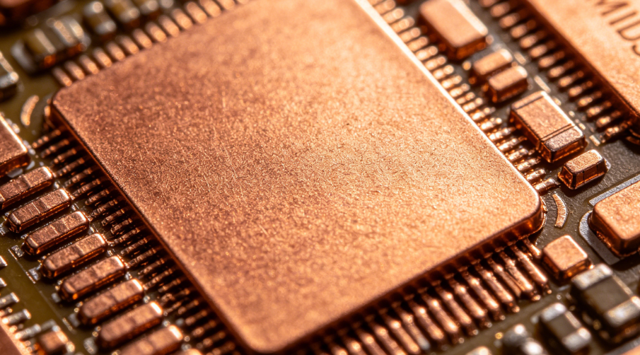
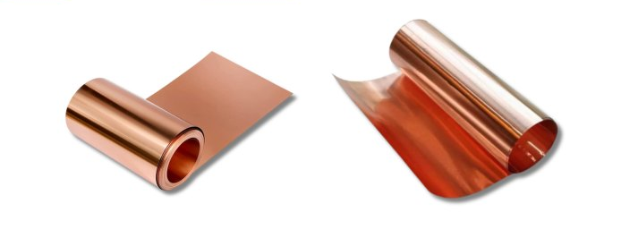
Copper foil is a thin, continuous sheet of high-purity copper produced for use in printed circuit boards. It acts as the conductive medium for traces, vias, and planes after etching and patterning. Manufacturers produce copper foil in various thicknesses, typically expressed in ounces per square foot, to match application needs. The foil's surface profile and grain structure directly affect adhesion, etchability, and electrical properties.
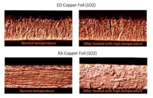
Two primary types dominate PCB applications: electrodeposited copper foil and rolled annealed copper foil. Electrodeposited copper foil forms through an electrolytic process where copper ions deposit onto a rotating drum, creating a foil with a shiny side and a rougher matte side. This design enhances bonding to substrates during lamination. Rolled annealed copper foil, by contrast, derives from mechanically rolling copper ingots followed by annealing to refine the grain structure, resulting in uniform smoothness on both sides.
IPC-4562 specifies classifications for these foils, including standard, high-temperature elongation, and low-profile variants to guide selection based on mechanical and electrical demands. Engineers specify foil type early in design to align with fabrication capabilities.
What Is Copper Cladding?
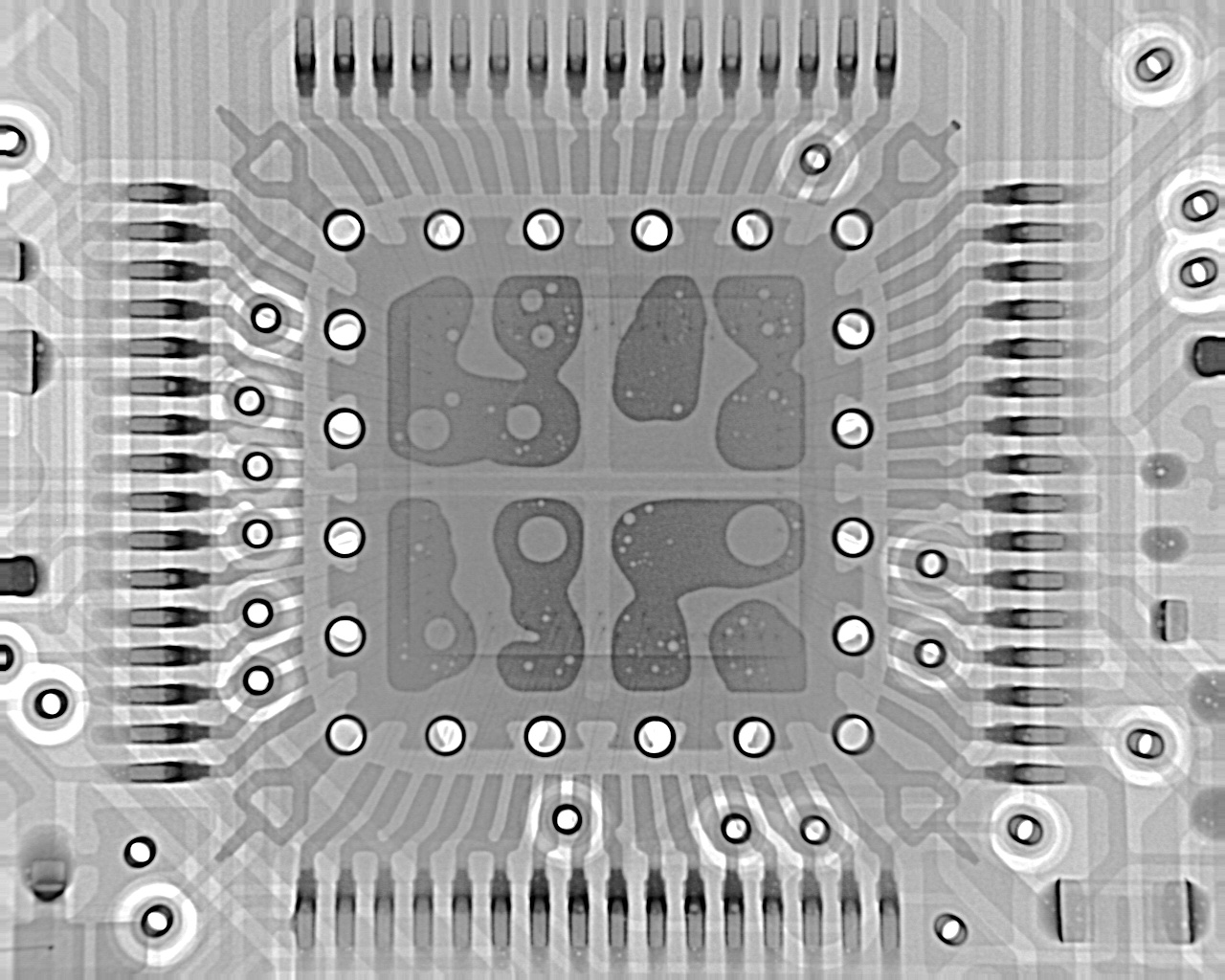
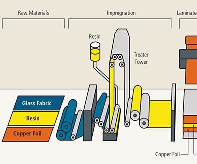
Copper cladding describes the composite material formed by bonding copper foil to one or both sides of a dielectric substrate, such as epoxy resin reinforced with glass fiber. This copper clad laminate (CCL) provides the foundational structure for rigid, flexible, or rigid-flex PCBs. The cladding process involves high-pressure, high-temperature lamination, ensuring strong interfacial adhesion between foil and core.
Cladding integrates the foil's properties with the substrate's insulation and mechanical support. Variations in foil type propagate to the clad laminate's performance, influencing peel strength and dimensional stability. In multilayer boards, inner layers use thinner cladding foils for finer lines and spaces.
The quality of copper cladding determines etch uniformity and via reliability. Standards like IPC-6012 outline qualification criteria for clad boards, emphasizing minimum copper thickness and surface quality post-processing. Proper cladding prevents delamination under thermal cycling.
Manufacturing Processes: From Foil to Cladding
Copper foil production begins with raw copper refinement to achieve high purity, critical for low resistivity. For electrodeposited foil, the electrolyte bath deposits copper at controlled rates, yielding thicknesses from 5 to 70 microns. Post-deposition, treatments like chemical roughening or oxide layers prepare the matte side for adhesion. Rolled annealed foil undergoes repeated rolling passes and heat treatment to achieve ductility without directional grain elongation.
Transitioning to cladding involves stacking foil, prepreg, and core materials in a press. Heat and pressure flow the resin, bonding layers while minimizing voids. Electrodeposited foil's tooth profile embeds into the resin for superior peel strength in rigid boards. Rolled annealed foil suits applications requiring bend radius without cracking, as in flexible circuits.
Process controls per IPC-4562 ensure foil profile consistency, directly impacting cladding integrity. Variations in foil grain orientation affect warpage during cooling.
Key Differences: Copper Foil vs. Copper Cladding
Copper foil exists as a standalone sheet, engineered for specific surface treatments and profiles before integration. Copper cladding, however, is the engineered laminate where foil properties interact with substrate characteristics. While foil dictates conductivity and etch response, cladding encompasses overall thickness, CTE matching, and thermal resistance.
In a copper foil vs copper cladding comparison, foil focuses on raw material attributes like ductility and roughness, whereas cladding emphasizes bonded performance metrics such as interlaminar bond strength. Electrodeposited foil excels in cost-effective rigid PCB cladding due to its adhesion profile. Rolled annealed foil enhances cladding for high-flex applications by reducing microcracks.
- Form: Copper foil = thin sheet; Copper cladding = laminated composite.
- Key properties: Copper foil = surface profile, grain structure; Copper cladding = peel strength, dielectric integration.
- Primary use: Copper foil = conductive layer precursor; Copper cladding = PCB base material.
- Types: Copper foil = ED, RA; Copper cladding = single/double-sided CCL.
These differences guide PCB materials comparison during stackup design. Foil selection influences cladding's response to plating and soldering.
Impact on PCB Performance
Copper foil type significantly affects PCB performance, particularly in signal propagation and reliability. Electrodeposited copper foil's rougher surface increases skin effect losses at high frequencies, elevating insertion loss in RF designs. Rolled annealed copper foil's smoother profile minimizes these losses, supporting gigabit speeds and low skew.
In thermal management, foil ductility influences via barrel integrity under reflow. RA foil resists cracking in dynamic flexing, vital for automotive or aerospace boards. Cladding uniformity ensures consistent impedance control across layers.
IPC-6012 performance specifications verify copper cladding's endurance through thermal shock and bend tests. Poor foil-to-substrate adhesion leads to paddle delamination in high-current paths. Engineers model these effects using foil profile data for accurate simulations.
High-density interconnects benefit from low-profile electrodeposited foils, bridging ED and RA advantages. Overall, PCB performance hinges on matching foil characteristics to operational stresses.
Best Practices for Selection in PCB Design
Select copper foil based on frequency, flex requirements, and cost constraints. For standard rigid boards below 1 GHz, electrodeposited copper foil provides reliable cladding at lower expense. High-speed designs above 10 GHz favor rolled annealed or low-profile variants to optimize skin depth.
Verify supplier compliance with IPC-4562 for foil grade and profile. During stackup, balance foil thickness with line width to maintain current capacity. Simulate warpage using CTE data from foil and substrate.
Test prototypes for peel strength and impedance per design rules. Collaborate with fabricators early to confirm cladding process compatibility. Document foil specs in fabrication drawings to avoid substitutions.
Incorporate margin for plating buildup, ensuring finished copper meets IPC-6012 minima.
Conclusion
Distinguishing copper foil from copper cladding clarifies their roles in PCB design, from raw conductivity to integrated reliability. Electrodeposited and rolled annealed copper foils offer tailored solutions for diverse applications, directly shaping PCB performance. By aligning selections with standards like IPC-4562 and IPC-6012, engineers achieve optimal signal integrity and durability. Prioritizing these differences enhances copper foil vs copper cladding decisions, driving robust PCB materials comparison.
FAQs
Q1: What are the main differences between electrodeposited copper foil and rolled annealed copper foil in PCB applications?
A1: Electrodeposited copper foil features a rough matte side for strong adhesion in rigid cladding, produced via electroplating for cost efficiency. Rolled annealed copper foil provides uniform smoothness and superior ductility, ideal for flexible PCBs and high-frequency performance. The choice impacts etch factor and skin effect losses, with ED suiting standard designs and RA enhancing bendability.
Q2: How does copper foil type affect PCB performance in high-speed designs?
A2: Smoother profiles like those in rolled annealed copper foil reduce surface roughness, minimizing dielectric and conductor losses for better signal integrity. Electrodeposited variants may introduce higher insertion loss due to tooth profiles. Engineers select based on frequency needs, ensuring cladding meets impedance targets.
Q3: Why is IPC-4562 important for copper foil vs copper cladding selection?
A3: IPC-4562 defines foil types, profiles, and treatments, ensuring consistency in PCB materials comparison. It guides qualification for electrodeposited and wrought foils, influencing cladding reliability. Compliance verifies performance under mechanical and thermal stress.
Q4: When should electric engineers prefer rolled annealed copper foil over electrodeposited?
A4: Opt for rolled annealed in flex or high-speed PCBs requiring low loss and fatigue resistance. Its isotropic grain supports tight bend radii without cracking. Electrodeposited suffices for rigid, cost-sensitive boards with good adhesion needs.
References
IPC-4562 — Metal Foil for Printed Circuit Boards. IPC
IPC-6012E — Qualification and Performance Specification for Rigid Printed Boards. IPC, 2017