 ALLPCB


In today’s fast-paced world of technology, High-Density Interconnect (HDI) printed circuit boards are at the heart of compact, high-performance devices like smartphones and advanced communications systems. If you’re wondering what HDI PCBs are and why they matter, here’s the quick answer: HDI PCBs are advanced circuit boards with higher wiring density, smaller vias, and finer lines, allowing for smaller, faster, and more efficient electronics. In this blog, we’ll dive deep into how HDI technology works, its benefits, and its critical role in modern devices. Let’s explore how this innovation is shaping the future of compact electronics.
What Are HDI Printed Circuit Boards?
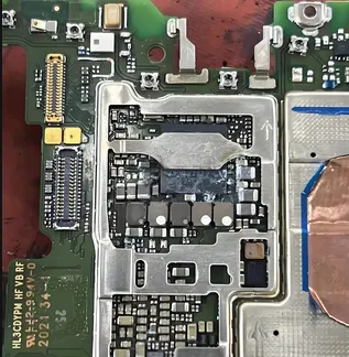
HDI stands for High-Density Interconnect, a type of printed circuit board (PCB) designed to pack more components into a smaller space. Unlike traditional PCBs, HDI boards use microvias, blind vias, and buried vias to create intricate connections between layers. This allows for finer line widths and spaces, often as small as 50 micrometers, compared to 150 micrometers or more in standard boards. The result is a compact board that can support complex circuits without sacrificing performance.
In devices like smartphones and communications systems, where space is limited, HDI PCBs are a game-changer. They enable manufacturers to build smaller, lighter products while maintaining high-speed signal transmission and reliability. With the rise of 5G technology and the demand for faster data transfer, HDI technology has become indispensable.
Key Features of HDI PCBs
HDI PCBs stand out due to several unique features that make them ideal for modern electronics. Here are the core characteristics that define their performance:
- Higher Circuit Density: HDI boards can accommodate more components per square inch thanks to their compact design. This is achieved through microvias (often less than 150 micrometers in diameter) and finer trace widths.
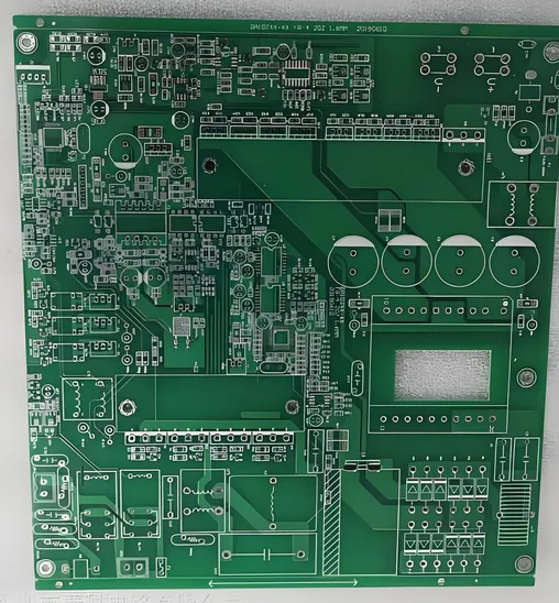
- Multi-Layer Construction: These boards often have 6 or more layers, with some advanced designs exceeding 20 layers, allowing for complex routing in a small footprint.
- Improved Signal Integrity: With shorter signal paths and reduced electromagnetic interference, HDI PCBs support high-speed data transfer, critical for 5G communications systems with signal speeds reaching up to 10 Gbps.
- Reduced Size and Weight: By minimizing the board size, HDI technology helps create slimmer devices, a must for modern smartphones that are often less than 8 mm thick.
These features make HDI PCBs a perfect fit for applications where performance and compactness are non-negotiable.
Why HDI PCBs Are Essential for Smartphones
Smartphones are a prime example of devices that rely heavily on HDI PCBs. With each new model, manufacturers aim to pack more features—better cameras, faster processors, and longer battery life—into smaller designs. HDI technology makes this possible by providing the following advantages:
1. Space Efficiency for Advanced Features
Modern smartphones often include multiple cameras, high-resolution displays, and powerful chipsets. HDI PCBs allow for dense component placement, fitting all these elements into a device that fits in your pocket. For instance, a typical smartphone motherboard using HDI technology can integrate over 100 components in an area smaller than 50 square centimeters.
2. Support for High-Speed Data
With the rollout of 5G, smartphones need to handle data speeds that demand precise signal routing. HDI PCBs minimize signal loss and crosstalk, ensuring that data transfer remains fast and reliable even at frequencies above 3 GHz.
3. Enhanced Battery Life
By reducing the size of the PCB, HDI designs leave more room for larger batteries or optimize power distribution. This contributes to better energy efficiency, a key selling point for devices that need to last a full day on a single charge.
The Role of HDI PCBs in Communications Systems
Beyond smartphones, HDI PCBs play a vital role in communications systems, including base stations, routers, and satellite equipment. As the backbone of global connectivity, these systems require high reliability and performance, areas where HDI technology excels.
1. Enabling 5G Infrastructure
5G networks operate at higher frequencies (up to 28 GHz in some cases) and require advanced hardware to manage signal integrity. HDI PCBs in base stations and antennas use controlled impedance traces (often around 50 ohms) to maintain signal quality over long distances. Their multi-layer design also supports the integration of multiple RF (radio frequency) components in a confined space.
2. Reliability in Harsh Environments
Communications equipment often operates outdoors, exposed to temperature fluctuations and humidity. HDI PCBs are built with robust materials like high-Tg (glass transition temperature) laminates, ensuring stability in conditions ranging from -40°C to 85°C.
3. Miniaturization of Networking Devices
From compact routers to portable satellite communicators, HDI PCBs allow for smaller, more efficient designs without compromising on functionality. This is crucial for deploying lightweight equipment in remote or mobile settings.
Benefits of HDI PCBs in Modern Electronics
The advantages of HDI PCBs extend across various industries, but their impact is especially notable in smartphones and communications systems. Here’s why this technology is a preferred choice for engineers and designers:
- Compact Design: HDI boards reduce the overall footprint, allowing for sleeker devices. This is evident in smartphones that have shrunk in thickness by nearly 50% over the past decade.
- Faster Performance: Shorter signal paths and reduced parasitic capacitance improve data rates, supporting applications like real-time video streaming at 4K resolution.
- Cost-Effective in the Long Run: While HDI PCBs may have higher upfront manufacturing costs due to precision requirements, their ability to integrate more functions into a single board reduces the need for additional components, saving money over time.
- Versatility: From consumer gadgets to industrial systems, HDI technology adapts to a wide range of applications, making it a flexible solution for complex designs.
Challenges in HDI PCB Design and Manufacturing
While HDI PCBs offer incredible benefits, they come with unique challenges that engineers must navigate during design and production. Understanding these hurdles can help in optimizing their use in smartphones and communications systems.
1. Complex Design Requirements
Designing an HDI board requires precision, as even a small error in trace spacing or via placement can lead to signal issues. Advanced software tools are often needed to simulate signal behavior and ensure impedance matching, especially for high-frequency applications like 5G.
2. Higher Manufacturing Costs
The use of microvias and fine traces demands specialized equipment and materials, increasing production costs. For example, laser drilling for microvias is more expensive than mechanical drilling used in traditional PCBs.
3. Thermal Management
With components packed closely together, heat dissipation becomes a concern. Engineers often incorporate thermal vias and heat sinks to manage temperatures, ensuring components operate within safe limits (typically below 85°C for most ICs).
How HDI PCBs Are Shaping the Future
As technology continues to evolve, HDI PCBs are poised to play an even bigger role in the future of electronics. Here are some trends to watch:
1. Integration with AI and IoT
With the growth of Artificial Intelligence (AI) and the Internet of Things (IoT), devices are becoming smarter and more connected. HDI PCBs will support the dense circuitry needed for AI processors and IoT sensors in compact forms, especially in smartphones that act as hubs for smart home systems.
2. Advancements in Materials
New materials with higher thermal conductivity and lower dielectric constants are being developed to enhance HDI performance. These innovations will further improve signal speeds and reliability in communications systems operating at frequencies beyond 30 GHz.
3. Sustainability in Manufacturing
The push for eco-friendly electronics is driving research into sustainable HDI PCB production. From using bio-based laminates to reducing waste during fabrication, the industry is aligning with global sustainability goals.
Why Choose HDI PCBs for Your Next Project?
For engineers and businesses working on cutting-edge smartphones or communications systems, HDI PCBs offer unmatched advantages in terms of size, speed, and reliability. Whether you’re designing a device to support 5G connectivity or a compact gadget with multiple features, this technology provides the foundation for success. Partnering with a trusted PCB provider ensures that you get high-quality HDI boards tailored to your specific needs, from prototype to mass production.
Conclusion
HDI printed circuit boards are transforming the landscape of modern electronics, especially in smartphones and communications systems. Their ability to pack more power into smaller spaces while maintaining high-speed performance makes them indispensable in today’s tech-driven world. From enabling 5G networks to supporting the latest smartphone innovations, HDI technology is paving the way for a connected, compact future. By understanding their features, benefits, and challenges, engineers can leverage HDI PCBs to create devices that meet the demands of tomorrow.
At ALLPCB, we’re committed to delivering top-notch HDI PCB solutions to bring your ideas to life. Whether you’re innovating in consumer electronics or building critical communications infrastructure, we’re here to support your journey with precision and expertise.


