ALLPCB


In the fast-evolving world of electronics, achieving higher performance in smaller spaces is a constant challenge. High-Density Interconnect (HDI) PCBs are the solution, especially when it comes to their inner layers. If you're wondering how HDI PCB inner layer microvias, blind and buried vias inner layer, and high-density routing inner layer contribute to better designs, you're in the right place. This blog dives deep into how these elements maximize density and performance, offering practical insights for engineers and designers looking to optimize their circuit board designs.
At its core, HDI technology allows for more components to fit into a smaller area by utilizing advanced techniques in the inner layers of a PCB. We'll explore the critical role of microvias, blind and buried vias, and high-density routing, breaking down their benefits and applications with specific details and examples. Let's get started.
What Are HDI PCBs and Why Do Inner Layers Matter?
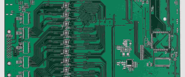
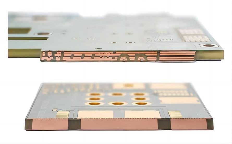
HDI PCBs are specialized circuit boards designed to pack more functionality into a smaller footprint. Unlike traditional PCBs, they feature finer lines, smaller vias, and denser connections, often requiring fewer layers to achieve the same or better performance. The inner layers of an HDI PCB are where much of this magic happens. These layers house complex routing and connections that are hidden from the outer surfaces, enabling compact designs for modern devices like smartphones, wearables, and medical equipment.
The inner layers are crucial because they provide additional space for routing signals and power without increasing the board's overall size. By leveraging technologies like HDI PCB inner layer microvias and blind and buried vias inner layer, designers can create intricate pathways for signals, ensuring high performance while maintaining a small form factor. In short, the inner layers are the backbone of HDI technology, allowing for greater density without sacrificing reliability or speed.
Understanding HDI PCB Inner Layer Microvias
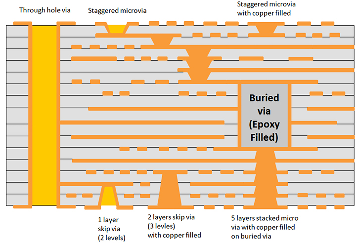
Microvias are tiny holes, often less than 150 micrometers in diameter, that connect different layers of a PCB. In HDI designs, these are typically laser-drilled for precision and are a game-changer for inner layer connections. Unlike traditional through-hole vias that pass through the entire board, HDI PCB inner layer microvias connect only adjacent layers, saving space and improving signal integrity.
For example, in a 10-layer HDI PCB, microvias might connect layer 2 to layer 3 or layer 8 to layer 9 without interfering with other layers. This targeted connection reduces the need for long vias, which can introduce signal delays or interference. With microvias, signal paths are shorter, often achieving transmission speeds that support high-frequency applications above 5 GHz, a critical factor for modern communication devices.
Additionally, microvias allow for a higher via density, sometimes up to 100 vias per square centimeter, enabling more connections in a smaller area. This is especially important in inner layers, where space is at a premium. However, designers must ensure proper aspect ratios—typically 1:1 or less for microvias—to maintain reliability during manufacturing and prevent issues like cracking under thermal stress.
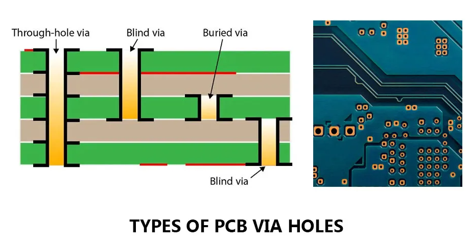
The Role of Blind and Buried Vias in Inner Layers
When it comes to maximizing space in HDI PCBs, blind and buried vias inner layer technology plays a pivotal role. These vias differ from standard through-hole vias because they don't extend through the entire board. Instead, they are strategically placed to connect specific layers, freeing up space for additional routing channels.
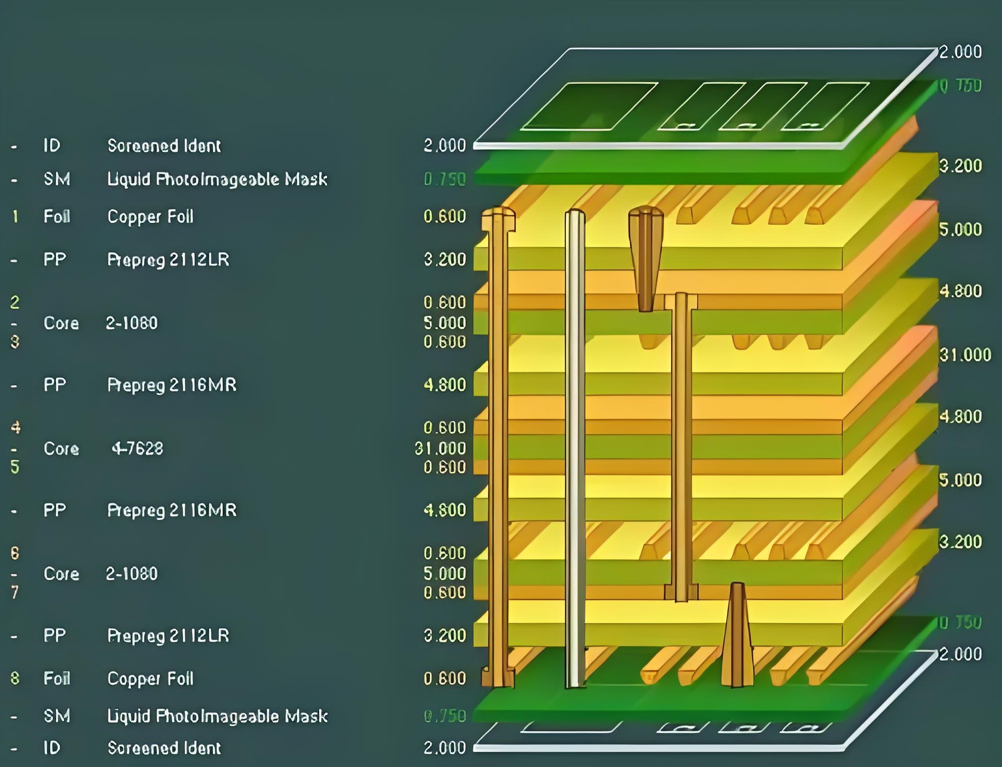
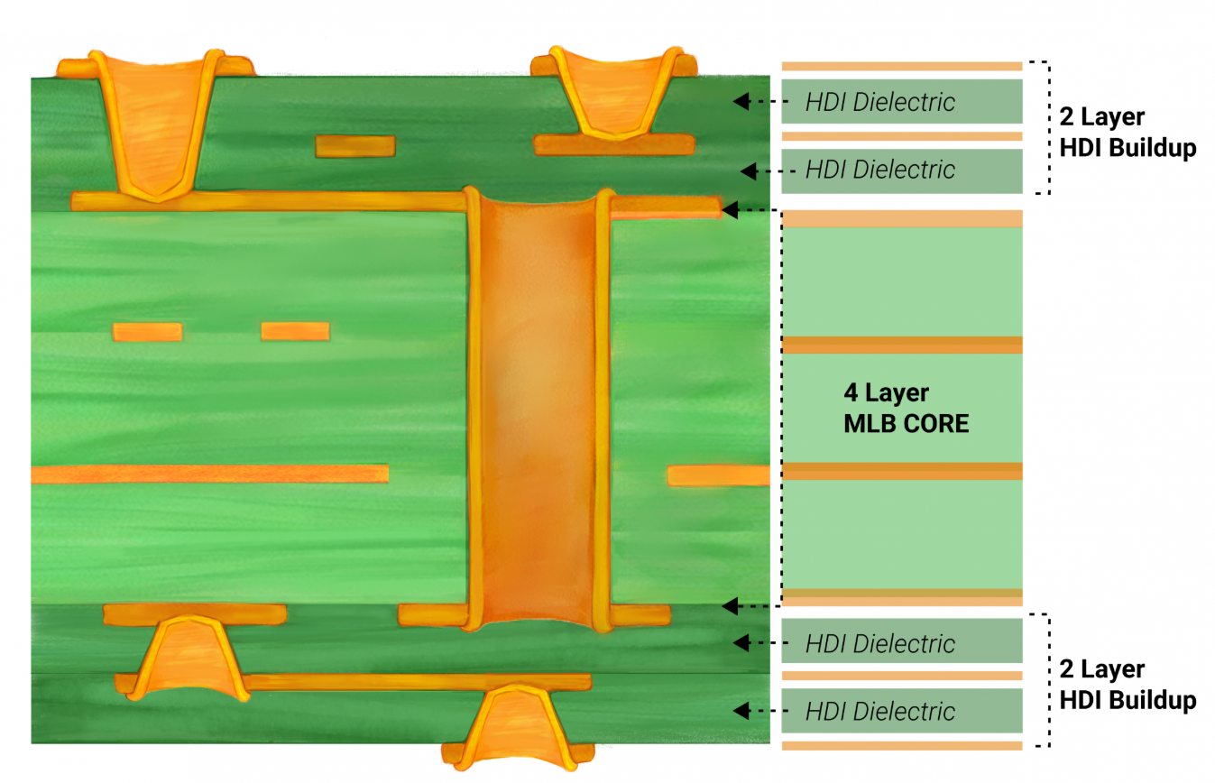
Blind vias connect an outer layer to one or more inner layers without passing through the entire board. For instance, a blind via might link layer 1 (the top surface) to layer 2, leaving the lower layers untouched. Buried vias, on the other hand, are completely hidden within the inner layers, connecting, say, layer 3 to layer 4 without reaching the surface. This approach is ideal for high-density routing inner layer designs, as it prevents vias from occupying valuable surface real estate needed for components.
The advantage of using blind and buried vias is clear in multi-layer designs. In a typical 8-layer HDI board, using these vias can reduce the number of signal layers needed by up to 30%, as they create more routing paths within the inner layers. This not only shrinks the board size but also lowers manufacturing costs by reducing layer count. Moreover, blind and buried vias improve signal integrity by minimizing stub effects—unwanted signal reflections that occur in longer vias—ensuring cleaner transmission for high-speed signals above 10 Gbps.
High-Density Routing in Inner Layers: The Key to Compact Designs
Routing is the process of creating pathways for electrical signals across a PCB, and in HDI designs, high-density routing inner layer techniques are essential for fitting more connections into limited space. Inner layers are often dedicated to routing critical signals, such as power distribution and high-speed data lines, away from the noise and interference that can occur on outer layers.
High-density routing involves using finer trace widths and spacing, often as small as 3 mils (0.076 mm) for both, compared to 6-8 mils in standard PCBs. This allows for more traces per unit area, sometimes doubling the routing capacity in inner layers. For instance, in a design supporting a high-performance processor, inner layer routing might handle hundreds of connections for data buses operating at frequencies up to 3 GHz, ensuring minimal crosstalk and impedance mismatch (typically maintained at 50 ohms for single-ended signals).
To achieve this level of density, designers often combine high-density routing with microvias and blind/buried vias. This combination creates a network of short, efficient signal paths within the inner layers, reducing latency and power loss. However, it requires precise control over impedance and careful layer stacking to avoid signal degradation. Advanced simulation tools are often used to predict and optimize these parameters before manufacturing.
Benefits of Optimizing Inner Layers in HDI PCBs
Focusing on the inner layers of HDI PCBs offers several advantages that directly impact performance and cost. Let's break down some of the key benefits:
- Space Efficiency: By using HDI PCB inner layer microvias and blind and buried vias inner layer, designers can fit more functionality into a smaller board area. This is critical for applications like mobile devices, where every millimeter counts.
- Improved Signal Integrity: Shorter signal paths and reduced via stubs in inner layers minimize noise and interference, supporting high-speed signals with frequencies exceeding 5 GHz and data rates above 10 Gbps.
- Reduced Layer Count: Efficient use of inner layers for high-density routing inner layer can cut down the total number of layers needed, sometimes by 20-30%, lowering production costs and board thickness.
- Enhanced Reliability: Inner layer connections are less exposed to environmental factors like moisture or mechanical stress, improving the long-term durability of the PCB.
These benefits make HDI PCBs with optimized inner layers a preferred choice for industries like telecommunications, automotive, and consumer electronics, where performance and compactness are non-negotiable.
Challenges in Designing HDI PCB Inner Layers
While the advantages are significant, designing HDI PCB inner layers comes with its own set of challenges. One major hurdle is manufacturing precision. Laser-drilling microvias with diameters below 100 micrometers requires advanced equipment, and even slight misalignments can lead to connection failures. Maintaining an aspect ratio of 0.8:1 or lower for microvias is often necessary to ensure reliability, but this can limit design flexibility.
Another challenge is thermal management. High-density routing in inner layers can lead to heat buildup, especially in designs with high-power components. Designers must incorporate thermal vias or heat-dissipating materials, which can complicate the layout. Additionally, signal integrity issues like crosstalk and impedance mismatches become more pronounced in dense inner layer designs, requiring meticulous planning and testing.
Cost is also a factor. The advanced techniques needed for HDI PCB inner layer microvias and blind and buried vias inner layer often increase manufacturing expenses, especially for small production runs. However, the trade-off is often worth it for applications where performance outweighs cost concerns.
Applications of HDI PCBs with Advanced Inner Layer Designs
The use of optimized inner layers in HDI PCBs has transformed several industries by enabling smaller, faster, and more reliable electronics. Here are some common applications:
- Consumer Electronics: Devices like smartphones and tablets rely on HDI PCBs to pack powerful processors, memory, and sensors into tiny spaces, with inner layers handling complex routing for data speeds up to 20 Gbps.
- Medical Devices: Wearable health monitors and implantable devices use HDI technology to achieve miniaturization, with inner layer microvias ensuring precise signal transmission for critical data.
- Automotive Systems: Modern vehicles incorporate HDI PCBs in control units and sensors, where high-density inner layer routing supports real-time processing with minimal latency.
- Telecommunications: High-frequency applications like 5G infrastructure depend on HDI inner layers to manage signals with low loss and high fidelity, often at frequencies above 28 GHz.
These examples highlight how inner layer optimization in HDI PCBs drives innovation across diverse fields, meeting the demands for performance and compactness.
Best Practices for Designing HDI PCB Inner Layers
To make the most of HDI technology, designers should follow certain best practices when working on inner layers. First, prioritize via placement by using blind and buried vias inner layer to free up surface space and reduce signal interference. Plan microvia locations early in the design process to avoid manufacturing issues, ensuring aspect ratios stay within safe limits (e.g., 1:1 or less).
Second, focus on impedance control for high-density routing inner layer designs. Match trace widths and dielectric materials to maintain consistent impedance, often around 50 ohms for high-speed signals, to prevent reflections. Use simulation tools to test signal integrity before finalizing the layout.
Lastly, collaborate closely with your manufacturing partner to understand their capabilities for microvia drilling and layer stacking. Specify tolerances clearly, as even a 10-micrometer deviation can affect performance in high-density designs. By adhering to these practices, you can achieve reliable, high-performing HDI PCBs tailored to your needs.
Conclusion: Unlocking the Full Potential of HDI PCB Inner Layers
HDI PCBs are revolutionizing electronics by enabling smaller, faster, and more efficient designs, and their inner layers are at the heart of this transformation. Through the strategic use of HDI PCB inner layer microvias, blind and buried vias inner layer, and high-density routing inner layer techniques, engineers can maximize density and performance, meeting the demands of cutting-edge applications.
From improving signal integrity with shorter paths to reducing board size with fewer layers, the benefits of optimizing inner layers are undeniable. While challenges like manufacturing precision and thermal management exist, following best practices and leveraging advanced design tools can overcome these hurdles. As technology continues to advance, the role of HDI PCB inner layers will only grow, powering the next generation of compact, high-performance devices.
Whether you're designing for consumer electronics, medical equipment, or automotive systems, understanding and utilizing the power of HDI inner layers is key to staying ahead. With the right approach, you can push the boundaries of what's possible in PCB design.