ALLPCB


In the fast-paced world of mobile phone technology, every component must be smaller, faster, and more efficient. High-Density Interconnect (HDI) PCBs play a crucial role in achieving this. But what exactly are HDI PCBs, and how do they contribute to the miniaturization and performance of mobile phones? Simply put, HDI PCBs use advanced techniques like microvia technology and high-density interconnects to pack more functionality into smaller spaces while maintaining superior signal integrity and speed. In this blog, we’ll dive deep into the advantages of HDI PCBs, explore microvia technology, and explain how mobile phone PCB layers and HDI stackup designs revolutionize modern devices. Let’s uncover the secrets behind these powerful circuit boards.
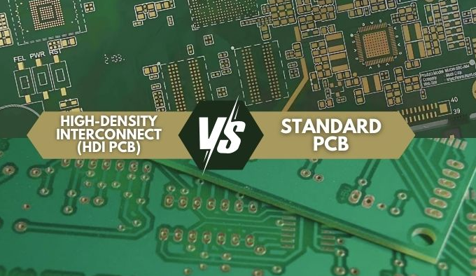
What Are HDI PCBs and Why Do They Matter in Mobile Phones?
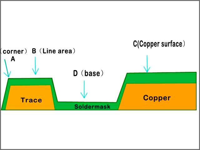
High-Density Interconnect (HDI) PCBs are specialized circuit boards designed to fit more components and connections into a smaller area. Unlike traditional PCBs, which rely on larger through-hole vias, HDI boards use microvias—tiny holes with diameters often less than 0.15 mm—to create connections between layers. This allows for denser routing and reduced board size, which is critical for compact devices like mobile phones.
In mobile phones, space is a premium. Every millimeter counts when fitting powerful processors, high-resolution cameras, and long-lasting batteries into a sleek design. HDI PCBs enable this by supporting complex circuits in a smaller footprint. Beyond size, they also improve performance by reducing signal loss and enhancing electrical efficiency, ensuring that your phone operates smoothly even during demanding tasks like gaming or streaming.
The Key Advantages of HDI PCBs in Mobile Phones
HDI PCBs offer several benefits that make them indispensable in mobile phone manufacturing. Let’s explore these HDI PCB advantages in detail:
1. Miniaturization for Sleeker Designs
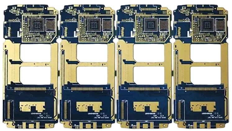
One of the standout benefits of HDI PCBs is their ability to reduce the overall size of the circuit board. By using microvias and finer trace widths (often as small as 0.075 mm), designers can stack more layers and components into a compact space. This directly translates to thinner and lighter mobile phones without sacrificing functionality. For instance, modern flagship phones often fit 8 to 12 layers of circuitry into a board less than 1 mm thick, thanks to HDI technology.
2. Improved Signal Integrity and Speed
In mobile phones, fast and reliable signal transmission is vital. HDI PCBs minimize signal interference by shortening the distance between components and reducing the length of interconnects. This results in lower impedance—often in the range of 50 to 100 ohms for high-speed signals—and faster data transfer rates, which are essential for 5G connectivity and high-performance apps.
3. Higher Component Density
With HDI PCBs, manufacturers can place more components on both sides of the board. This high-density interconnect capability supports the integration of advanced features like multiple cameras, AI processors, and enhanced sensors in a single device. It’s not uncommon for a mobile phone PCB to house over 1,000 components in a space smaller than a credit card.
4. Enhanced Reliability
The use of microvias and advanced materials in HDI PCBs reduces the risk of mechanical failure. These boards are designed to withstand the constant vibrations and temperature changes that mobile phones endure, ensuring long-term durability even in rugged conditions.
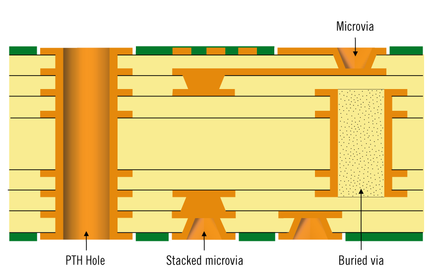
Microvia Technology: The Backbone of HDI PCBs
At the heart of HDI PCB design lies microvia technology. Microvias are small, laser-drilled holes that connect different layers of a circuit board. Unlike traditional vias, which can be as large as 0.8 mm in diameter, microvias are typically 0.1 to 0.15 mm, allowing for much denser layouts. Here’s why microvia technology is a game-changer for mobile phones:
- Space Efficiency: Microvias take up less surface area, freeing up space for additional components or smaller board designs.
- Layer Stacking: They enable the creation of multilayer boards with intricate HDI stackups, often exceeding 10 layers in premium mobile devices.
- Better Electrical Performance: Shorter microvias reduce signal delay and parasitic capacitance, improving overall performance. For example, signal propagation delay can be reduced by up to 30% compared to traditional vias.
Microvia technology also supports blind and buried vias, which are vias that don’t pass through the entire board. This further optimizes space and enhances design flexibility, making it possible to create highly compact yet powerful mobile phone circuits.
Understanding Mobile Phone PCB Layers and HDI Stackup
Mobile phone PCB layers refer to the number of conductive layers within a circuit board, each separated by insulating material. Traditional PCBs might have 2 to 4 layers, but HDI PCBs in mobile phones often feature 8 to 14 layers or more. The arrangement of these layers, known as the HDI stackup, is critical for balancing size, performance, and manufacturability.
Why Multiple Layers Matter
Each layer in an HDI PCB serves a specific purpose, such as power distribution, grounding, or signal routing. By increasing the number of layers, designers can separate high-speed signals from power lines, reducing interference and noise. For example, a typical mobile phone PCB might dedicate one layer to 5G antenna signals while using another for grounding to maintain signal integrity.
HDI Stackup Design for Performance
The HDI stackup design determines how layers are arranged and connected using microvias. A well-designed stackup minimizes signal crosstalk and ensures efficient heat dissipation—a key concern in mobile phones where components like processors can reach temperatures of 40-50°C during heavy use. Common stackup configurations in mobile phones include 1+N+1 or 2+N+2, where “N” represents the core layers, and the numbers indicate additional build-up layers on each side.
How HDI PCBs Drive Miniaturization in Mobile Phones
Miniaturization is the cornerstone of modern mobile phone design, and HDI PCBs are the key enablers. By leveraging high-density interconnects and microvia technology, these boards allow manufacturers to shrink device sizes while packing in more features. Here’s how:
- Reduced Board Size: HDI PCBs can cut board dimensions by up to 60% compared to traditional designs, as noted in industry insights. This allows for slimmer phone profiles, often under 8 mm thick.
- Support for Smaller Components: With finer traces and smaller vias, HDI PCBs accommodate tiny surface-mount components, such as 0201-sized resistors and capacitors, which are just 0.6 mm by 0.3 mm.
- Integration of Advanced Features: The compact nature of HDI PCBs makes room for larger batteries or additional modules like wireless charging coils without increasing the phone’s size.
The result? Mobile phones that are not only smaller and lighter but also more powerful, meeting consumer demands for portability and performance.
Performance Secrets: How HDI PCBs Enhance Mobile Phone Functionality
Beyond miniaturization, HDI PCBs unlock performance improvements that elevate the user experience. Let’s break down how they achieve this:
1. Support for High-Speed Connectivity
With the rise of 5G and Wi-Fi 6, mobile phones need to handle data rates exceeding 1 Gbps. HDI PCBs are designed to support these speeds by minimizing signal loss through optimized trace layouts and controlled impedance, often maintained at 50 ohms for RF signals.
2. Efficient Power Management
Mobile phones rely on efficient power distribution to maximize battery life. HDI PCBs use dedicated power and ground planes in their stackup to reduce voltage drops and ensure stable power delivery, even during peak usage when current draw can spike to 2-3 amps.
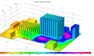
3. Thermal Management
High-performance components generate heat, and HDI PCBs help manage this through strategic layer design and the use of thermal vias. These vias conduct heat away from critical components, preventing overheating and maintaining performance during extended use.
Applications of HDI PCBs Beyond Mobile Phones
While this blog focuses on mobile phones, it’s worth noting that the benefits of HDI PCBs extend to other industries. They are widely used in wearable devices, medical equipment, and automotive electronics, where compactness and reliability are equally important. The same principles of high-density interconnects and microvia technology apply, demonstrating the versatility of HDI designs.
Challenges in HDI PCB Design and Manufacturing
Despite their advantages, HDI PCBs come with unique challenges. The manufacturing process is more complex due to the precision required for microvias and fine traces. Laser drilling for microvias, for instance, demands high accuracy to avoid defects, and the cost of materials like high-frequency laminates can be significant. Additionally, designing an effective HDI stackup requires careful planning to balance electrical performance with thermal and mechanical constraints.
However, advancements in manufacturing technology continue to address these challenges, making HDI PCBs more accessible for a wide range of applications, including mobile phones.
Conclusion: The Future of HDI PCBs in Mobile Phones
HDI PCBs are the unsung heroes behind the sleek, powerful mobile phones we use every day. Through innovations like microvia technology and high-density interconnects, they enable miniaturization without compromising performance. As mobile technology evolves with trends like foldable displays and 6G connectivity, the role of HDI PCBs will only grow, pushing the boundaries of what’s possible in compact electronics.
Understanding the intricacies of mobile phone PCB layers and HDI stackup designs reveals just how much thought goes into every device. Whether it’s achieving faster data speeds, extending battery life, or fitting more features into a smaller frame, HDI PCBs are at the forefront of mobile phone innovation. At ALLPCB, we’re committed to supporting this progress by providing cutting-edge solutions for your circuit board needs, ensuring that your designs are ready for the future.