 ALLPCB


In the fast-paced world of electronics, High-Density Interconnect (HDI) PCBs are at the forefront of innovation, enabling smaller, faster, and more efficient devices. But how do manufacturers ensure that these complex boards meet the highest standards of quality and reliability? The answer lies in adhering to strict guidelines, particularly the IPC standards for HDI PCB design and manufacturing, such as IPC-2226. In this blog, we’ll dive deep into what HDI PCB IPC standards entail, explore the specifics of IPC-2226 for HDI PCB, and outline the key HDI PCB manufacturing standards to ensure compliance and top-notch quality.
Whether you're an engineer designing cutting-edge technology or a manufacturer aiming to produce reliable boards, understanding these standards is critical. Let’s explore the essentials of HDI PCB compliance and how they impact the production process.
What Are HDI PCBs and Why Do Standards Matter?
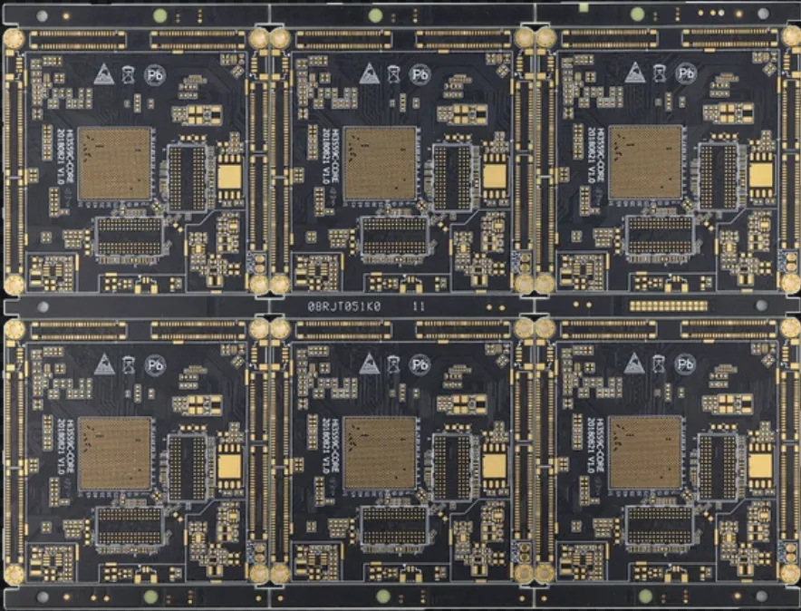
HDI PCBs are advanced printed circuit boards designed to pack more components into a smaller space. They achieve this through finer traces, smaller vias (like microvias), and higher layer counts compared to traditional PCBs. These boards are essential for modern electronics, such as smartphones, medical devices, and aerospace systems, where space and performance are critical.
However, the complexity of HDI PCBs introduces unique challenges in design and manufacturing. Without strict guidelines, issues like signal interference, thermal stress, or manufacturing defects can compromise the board’s performance. This is where IPC standards come in. Developed by the Institute of Printed Circuits (IPC), these standards provide a framework for designing and producing reliable HDI PCBs. They ensure consistency, quality, and compatibility across industries, making compliance non-negotiable for manufacturers and designers alike.
Understanding HDI PCB IPC Standards
The IPC standards are a set of guidelines and specifications that cover every aspect of PCB design, manufacturing, and testing. For HDI PCBs, these standards address the unique requirements of high-density layouts, ensuring that boards can handle high-speed signals and compact designs without failure. Let’s break down the key IPC standards relevant to HDI PCBs.
IPC-2221: Generic Standard on Printed Board Design
IPC-2221 serves as the foundation for PCB design, including HDI boards. It provides general guidelines on aspects like trace width, spacing, and material selection. For HDI designs, this standard helps engineers determine safe electrical clearances and insulation requirements to prevent issues like crosstalk or short circuits in densely packed layouts.
For example, in an HDI PCB with a trace width of 3 mils (0.076 mm), IPC-2221 ensures that the spacing between traces is sufficient to avoid electrical interference, often recommending a minimum of 3 mils for standard voltages. Following these rules is crucial for maintaining signal integrity in high-speed applications.
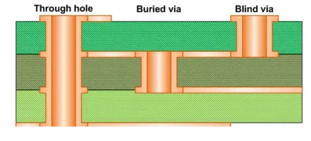
IPC-2226: Sectional Design Standard for HDI PCBs
The IPC-2226 standard is specifically tailored for HDI PCB design. It defines the requirements for high-density interconnect structures, focusing on microvias, blind vias, and buried vias. This standard categorizes HDI designs into different types based on their complexity and via structures:
- Type I: Features microvias with a diameter of 0.15 mm (6 mils) or less, typically used in less complex HDI boards.
- Type II: Includes blind vias that don’t pass through the entire board, allowing for denser routing.
- Type III: Combines stacked microvias and buried vias for highly complex designs with multiple layers.
IPC-2226 also provides guidelines on aspect ratios for vias, recommending a maximum ratio of 0.75:1 for microvias to ensure reliable plating and structural integrity during manufacturing. Adhering to these specifications helps reduce defects like via cracking, which can occur under thermal stress in compact designs.
IPC-6012: Qualification and Performance Specification
While IPC-2226 focuses on design, IPC-6012 addresses the manufacturing and performance requirements for rigid PCBs, including HDI boards. It sets criteria for aspects like copper thickness, solder mask adhesion, and thermal reliability. For HDI PCBs, compliance with IPC-6012 ensures that the board can withstand the stresses of assembly and operation, especially in high-density configurations where heat dissipation is a concern.
For instance, IPC-6012 specifies a minimum copper thickness of 0.5 oz/ft2 (17.5 μm) for internal layers in HDI designs to maintain conductivity without overheating. This is vital for applications where signal speeds can reach up to 5 GHz or more, as seen in advanced communication devices.
Key HDI PCB Manufacturing Standards
Manufacturing HDI PCBs is a complex process that requires precision at every step. The following HDI PCB manufacturing standards, often aligned with IPC guidelines, are critical to producing high-quality boards.
Material Selection for HDI PCBs
HDI boards often require specialized materials to handle high frequencies and thermal loads. IPC standards recommend using high-Tg (glass transition temperature) materials, such as FR-4 with a Tg of 170°C or higher, to prevent warping during soldering processes like reflow at temperatures around 260°C. Additionally, low-loss dielectric materials with a dissipation factor (Df) of 0.005 or less are preferred for high-speed signals to minimize signal loss.
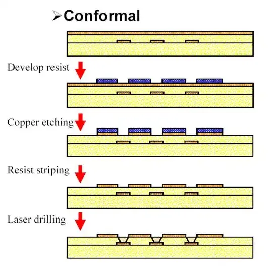
Precision in Via Formation
Forming microvias, blind vias, and buried vias is a cornerstone of HDI PCB manufacturing. IPC-2226 mandates tight tolerances for via drilling and plating to avoid defects. For example, laser drilling is often used to create microvias with diameters as small as 0.1 mm (4 mils), and the plating process must achieve a uniform copper thickness of at least 20 μm to ensure reliable connections.
Manufacturers must also control the aspect ratio during via formation. A high aspect ratio (e.g., above 1:1) can lead to incomplete plating, causing open circuits. Following IPC guidelines helps maintain a balance between density and manufacturability.
Layer Stackup and Signal Integrity
HDI PCBs often feature multiple layers—sometimes 8 or more—to accommodate dense routing. IPC standards guide the stackup design to ensure signal integrity and impedance control. For instance, maintaining a controlled impedance of 50 ohms (±10%) for high-speed signals requires precise layer spacing and dielectric thickness, often around 0.1 mm (4 mils) between critical layers.
Manufacturers must also consider crosstalk by ensuring adequate spacing between high-speed traces, typically at least 3 times the trace width as per IPC-2221 recommendations. Proper stackup design minimizes electromagnetic interference (EMI), which is crucial for applications like 5G devices operating at frequencies above 3 GHz.
Testing and Quality Assurance
Quality control is a vital part of HDI PCB manufacturing standards. IPC-6012 outlines testing methods like microsection analysis to inspect via integrity and plating quality. Automated Optical Inspection (AOI) and X-ray testing are also used to detect defects in microvias or misaligned layers, ensuring that the board meets performance criteria before assembly.
For example, thermal cycling tests, as per IPC-TM-650, expose the board to temperature swings between -40°C and 125°C to simulate real-world conditions. Passing these tests confirms that the HDI PCB can endure operational stress without delamination or via failure.
Benefits of Adhering to HDI PCB IPC Standards
Following HDI PCB IPC standards offers several advantages for both designers and manufacturers. Here are some key benefits:
- Improved Reliability: Compliance with standards like IPC-2226 and IPC-6012 ensures that HDI PCBs can withstand harsh environments, reducing failure rates in critical applications like medical equipment.
- Enhanced Performance: Proper design and manufacturing practices maintain signal integrity, supporting high-speed data transfer rates up to 10 Gbps or more in modern devices.
- Cost Efficiency: While HDI PCBs are more expensive to produce, adhering to standards minimizes rework and defects, saving costs in the long run.
- Global Compatibility: IPC standards are recognized worldwide, ensuring that HDI PCBs meet the requirements of international markets and industries.
Challenges in Meeting HDI PCB Manufacturing Standards
Despite the benefits, achieving compliance with HDI PCB manufacturing standards can be challenging. The precision required for microvia drilling and fine-line etching demands advanced equipment and skilled technicians. For instance, maintaining a line width of 2 mils (0.05 mm) with a tolerance of ±10% requires state-of-the-art photolithography tools, which can be costly.
Additionally, the use of advanced materials for high-frequency applications increases production expenses. Balancing cost with quality often requires manufacturers to invest in rigorous process controls and continuous training to meet IPC specifications.
How to Ensure Compliance with IPC Standards for HDI PCBs
For engineers and manufacturers looking to produce compliant HDI PCBs, here are practical steps to follow:
- Collaborate Early: Work closely with design and manufacturing teams during the initial stages to align on IPC-2226 guidelines for via types and stackup configurations.
- Use Advanced Tools: Leverage design software that incorporates IPC standards to simulate signal integrity and impedance before manufacturing.
- Conduct Thorough Testing: Implement IPC-recommended tests like thermal cycling and microsection analysis to validate board quality at every stage.
- Stay Updated: Regularly review updates to IPC standards, as technology evolves rapidly, and new guidelines may impact HDI PCB design and production.
Conclusion: Building Better HDI PCBs with IPC Standards
HDI PCBs are the backbone of modern electronics, enabling the compact, high-performance devices we rely on daily. However, their complexity demands strict adherence to HDI PCB IPC standards like IPC-2226 to ensure quality and reliability. From precise via formation to controlled impedance and rigorous testing, following these HDI PCB manufacturing standards is essential for success in today’s competitive market.
By understanding and implementing guidelines such as IPC-2226 for HDI PCB design, manufacturers can produce boards that meet the highest industry benchmarks. Whether you're designing for consumer electronics or critical aerospace systems, compliance with these standards guarantees that your HDI PCBs will perform flawlessly under any conditions. Trust in the process, invest in quality, and let IPC standards guide your path to innovation.


