 ALLPCB


Are you curious about how the heart of your favorite consumer electronics, like smartphones and smartwatches, comes to life? The journey from a concept to a fully functional device hinges on the intricate process of PCB manufacturing. In this comprehensive guide, we’ll walk you through the essential PCB manufacturing steps, the detailed PCB fabrication process, and provide a practical PCB assembly guide with a focus on SMT assembly for consumer electronics. Whether you're an engineer, a hobbyist, or a business looking to bring a product to market, understanding this process is key to ensuring quality and efficiency.
At ALLPCB, we’re passionate about making electronics manufacturing accessible and efficient. Let’s dive into the step-by-step journey of turning a design into a device, breaking down complex concepts into clear, actionable insights.
What Is PCB Manufacturing and Why Does It Matter for Consumer Electronics?
Printed Circuit Boards (PCBs) are the backbone of nearly every electronic device. They provide the physical platform where components like resistors, capacitors, and microchips are mounted and connected via conductive pathways. In consumer electronics, where devices need to be compact, lightweight, and reliable, the PCB manufacturing process plays a critical role in determining the performance and durability of the final product.
The process involves two main phases: fabrication, where the bare board is created, and assembly, where components are added to make it functional. Each phase requires precision to meet the high standards of modern electronics, ensuring signal integrity (often maintaining impedance values around 50-100 ohms for high-speed circuits) and minimizing delays (with signal speeds often exceeding 100 MHz in advanced designs).
Step 1: Design and Preparation – Laying the Foundation
Every PCB starts with a design. Engineers use specialized software to create a schematic, which is a blueprint of how components will connect. This schematic is then translated into a layout that maps out the physical placement of components and traces on the board.
During this stage, Design for Manufacturability (DFM) principles are applied to ensure the board can be produced efficiently. For instance, trace widths are calculated to handle specific current loads (e.g., 0.5 mm for 1A of current in standard designs), and spacing is set to avoid signal interference. Once the design is finalized, it’s exported as Gerber files—a universal format used by manufacturers to interpret the layout.
This step is crucial for consumer electronics, where compact designs often mean multi-layer boards (sometimes 4-12 layers) to fit complex circuitry into small spaces.
Step 2: PCB Fabrication Process – Building the Bare Board
The PCB fabrication process transforms the digital design into a physical board. This multi-step procedure requires precision to ensure the board meets electrical and mechanical requirements. Here’s how it works:
2.1 Material Selection
The base material, often FR-4 (a fiberglass-epoxy composite), is chosen for its durability and electrical insulation properties. For high-frequency consumer electronics, materials like Rogers or PTFE may be used to support signal speeds above 1 GHz.
2.2 Copper Cladding and Etching
A thin layer of copper is laminated onto the base material. Using the Gerber files, a photoresist layer is applied and exposed to UV light through a mask to define the circuit pattern. Unwanted copper is etched away with chemicals, leaving behind the conductive traces.
2.3 Drilling and Plating
Holes are drilled for mounting components and creating vias (connections between layers). These holes are plated with copper to ensure electrical conductivity across layers, critical for multi-layer boards in devices like tablets.
2.4 Solder Mask and Silkscreen
A protective solder mask is applied to prevent short circuits and corrosion, typically in green, though other colors are available. A silkscreen layer adds labels for component placement, aiding assembly.
At the end of fabrication, the bare board is ready for testing to check for defects like open circuits or misaligned layers before moving to assembly.
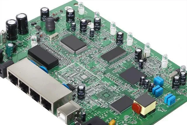
Step 3: PCB Assembly Guide – Bringing the Board to Life
Once the bare board is fabricated, the next phase is assembly, where electronic components are mounted and soldered. The PCB assembly guide below outlines the process, with a focus on techniques used in consumer electronics.
3.1 Component Sourcing and Preparation
Components like resistors, capacitors, and integrated circuits (ICs) are sourced based on the Bill of Materials (BOM) from the design phase. In consumer electronics, components are often miniaturized, with sizes as small as 0201 (0.6 mm x 0.3 mm), requiring precise handling.
3.2 Solder Paste Application
For Surface Mount Technology (SMT), a stencil is used to apply solder paste—a mix of tiny solder particles and flux—onto the board’s pads where components will be placed. This step ensures a strong bond during soldering.
3.3 Component Placement
Automated pick-and-place machines position components onto the board at high speeds, often placing thousands of components per hour. Accuracy is critical, as misalignment can lead to connection failures, especially in dense designs like those in smartphones.
3.4 Reflow Soldering
The board passes through a reflow oven, where controlled heat (typically peaking at 220-250°C) melts the solder paste, bonding components to the board. Cooling solidifies the connections, ensuring reliability.
Step 4: SMT Assembly for Consumer Electronics – Precision at Its Core
SMT assembly for consumer electronics is the dominant method due to its ability to support compact, high-density designs. Unlike Through-Hole Technology (THT), where components have leads inserted into holes, SMT mounts components directly onto the board’s surface, saving space and improving performance.
In SMT assembly, advanced techniques like Ball Grid Array (BGA) packaging are common for ICs in devices like gaming consoles. BGAs use tiny solder balls (often 0.4-0.8 mm in diameter) under the component, allowing hundreds of connections in a small footprint. However, this requires precise placement and X-ray inspection to verify solder joint quality.
SMT also enables faster production cycles, with assembly lines handling up to 50,000 components per hour, making it ideal for high-volume consumer electronics manufacturing.
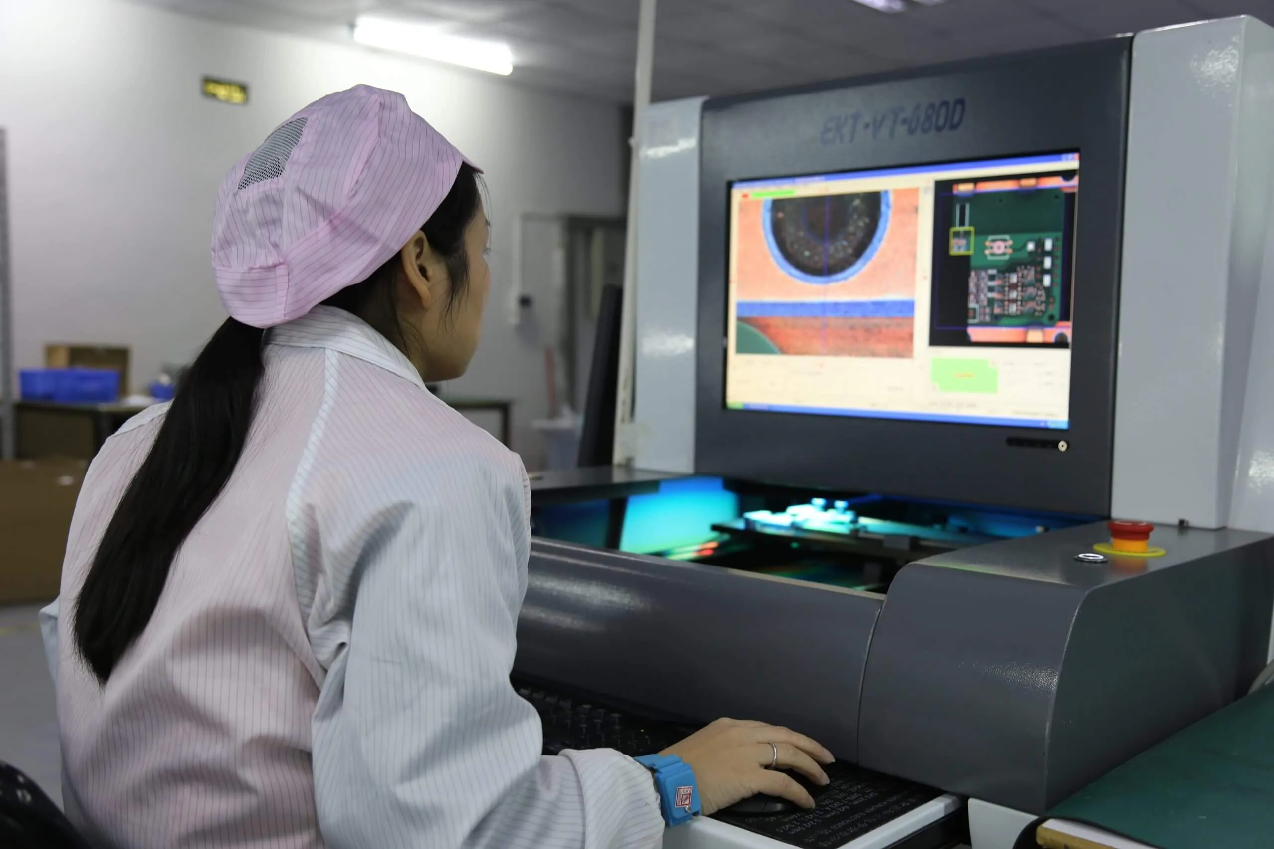
Step 5: Testing and Quality Assurance – Ensuring Reliability
After assembly, rigorous testing ensures the PCB functions as intended. Common tests include:
- In-Circuit Testing (ICT): Checks for electrical continuity and component functionality using probes.
- Functional Testing (FCT): Simulates real-world usage to verify the board performs its intended tasks.
- Automated Optical Inspection (AOI): Uses cameras to detect soldering defects or misplaced components.
For consumer electronics, additional environmental tests like temperature cycling (e.g., -40°C to 85°C) and humidity exposure ensure durability under various conditions. Only boards that pass these stringent checks move to the final integration into devices.
Step 6: Final Integration and Packaging – Ready for the Market
Once tested, the assembled PCB is integrated into the device’s housing, whether it’s a smartwatch, wireless earbuds, or a home automation hub. Connectors, cables, and other mechanical parts are added to complete the product. The final device undergoes further testing to ensure all systems work seamlessly together.
Packaging is the last step, designed to protect the product during shipping while providing an appealing unboxing experience for consumers. At this stage, manufacturers also ensure compliance with industry standards like RoHS (Restriction of Hazardous Substances) to meet global regulations.
Challenges in PCB Manufacturing for Consumer Electronics
Manufacturing PCBs for consumer electronics comes with unique challenges. Miniaturization demands tighter tolerances, often requiring trace widths as small as 0.1 mm. High-speed signals in devices like 5G smartphones need precise impedance control (e.g., 50 ohms for RF circuits) to prevent data loss. Additionally, cost pressures in competitive markets push manufacturers to optimize processes without compromising quality.
Advanced manufacturing techniques, such as laser drilling for micro-vias (diameters below 0.15 mm) and the use of flexible PCBs for wearable devices, help address these challenges, though they require specialized equipment and expertise.
How ALLPCB Supports Your PCB Manufacturing Journey
At ALLPCB, we streamline the entire process from design to device with end-to-end solutions. Our expertise in PCB manufacturing steps and PCB fabrication process ensures high-quality boards tailored to the demands of consumer electronics. Whether you need a prototype or high-volume production, our services cover everything from material selection to SMT assembly for consumer electronics, backed by rigorous testing and fast turnaround times.
Our user-friendly platform allows you to upload designs, get instant quotes, and track production in real-time. With a commitment to precision and customer satisfaction, we’re here to help bring your innovative ideas to life.
Conclusion: Turning Ideas into Reality
The journey from design to device is a fascinating blend of creativity and technical precision. By understanding the PCB manufacturing steps, diving deep into the PCB fabrication process, and following a reliable PCB assembly guide, you can ensure your consumer electronics meet the highest standards of quality and performance. With SMT assembly for consumer electronics driving innovation, the possibilities for smaller, faster, and smarter devices are endless.


