ALLPCB


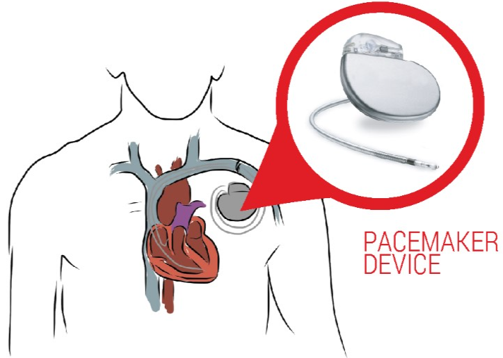
In the world of medical technology, pacemakers are life-saving devices that regulate heartbeats for millions of patients. As these devices become smaller and more advanced, the need for cutting-edge electronics has grown. High-Density Interconnect (HDI) PCB technology plays a vital role in making pacemakers more compact, reliable, and efficient. But what exactly are the HDI PCB benefits for pacemakers, and how do features like microvias, sequential lamination, and advanced routing techniques contribute to better designs? This blog dives deep into the role of HDI PCBs in pacemaker technology, exploring their advantages and the specific methods that make them ideal for medical implants.
At its core, HDI PCB technology allows for higher circuit density in a smaller space, which is critical for devices like pacemakers that must fit inside the human body. By using techniques such as microvias in pacemaker designs and via-in-pad technology for pacemakers, manufacturers can create intricate, reliable circuits. Let’s explore how these innovations, along with sequential lamination PCB for medical implants and advanced routing techniques for HDI PCBs, are transforming the field of medical electronics.
What is HDI PCB Technology?
High-Density Interconnect (HDI) PCBs are advanced printed circuit boards designed to pack more components and connections into a smaller area. Unlike traditional PCBs, HDI boards use finer lines, smaller vias, and multiple layers to achieve higher density. This is done through specialized manufacturing processes that allow for precise placement of components and interconnections.
In the context of pacemakers, HDI technology is a game-changer. These devices require circuits that are not only small but also highly reliable, as any failure could be life-threatening. HDI PCBs meet these demands by offering improved signal integrity, reduced power consumption, and the ability to integrate complex functionalities into a tiny footprint.
Key HDI PCB Benefits for Pacemakers
The use of HDI PCBs in pacemakers brings several advantages that directly impact the performance and safety of these critical devices. Here are some of the standout benefits:
- Compact Size: Pacemakers must be small enough to implant comfortably inside the body. HDI PCBs allow for a significant reduction in size—often up to 60% smaller than traditional boards—by stacking multiple layers and using microvias. This compact design is essential for minimally invasive implantation procedures.
- Enhanced Reliability: With finer traces and tighter spacing, HDI PCBs reduce the risk of signal interference and crosstalk. For pacemakers, this means more accurate monitoring and delivery of electrical pulses to the heart, with typical signal integrity improvements of up to 30% compared to older PCB designs.
- Lower Power Consumption: Pacemakers rely on batteries that need to last for years. HDI PCBs optimize power usage by minimizing resistance and capacitance in the circuit, extending battery life by as much as 20% in some designs.
- Improved Functionality: The high density of HDI boards allows for the integration of advanced features like wireless communication and real-time data monitoring, which are becoming standard in modern pacemakers.
These benefits make HDI PCBs the go-to choice for medical implants, ensuring that pacemakers are not only effective but also safe for long-term use.
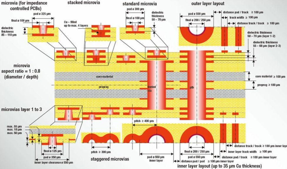
Microvias in Pacemaker Designs: Precision at a Micro Scale
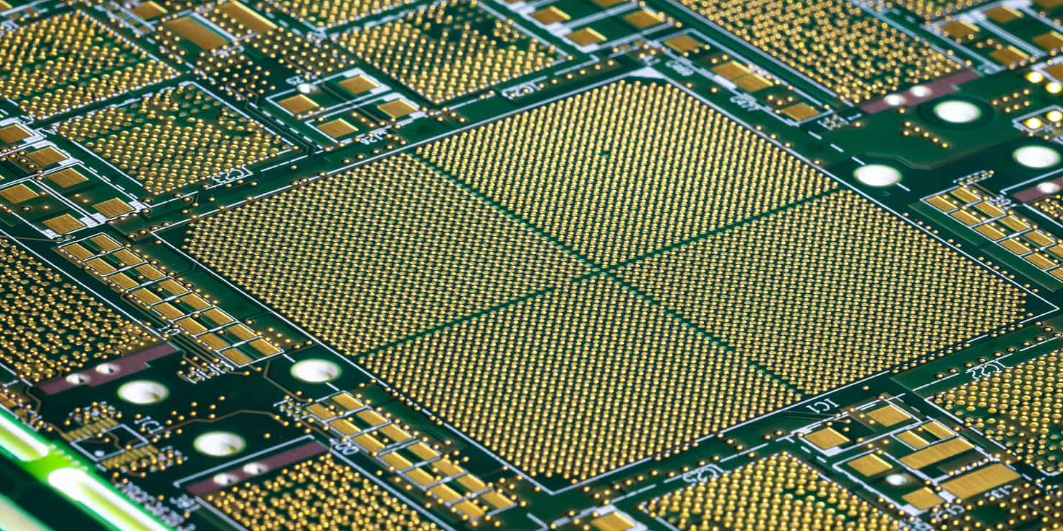
One of the defining features of HDI PCBs is the use of microvias—tiny holes that connect different layers of the board. In traditional PCBs, larger vias take up more space and limit the density of connections. Microvias, with diameters as small as 0.1 mm, allow for much tighter spacing and more connections in a smaller area.
For pacemaker designs, microvias in pacemaker designs are critical. They enable the creation of multi-layered boards where each layer can carry different signals or power levels without interference. This is particularly important for pacemakers, which often need to process complex signals at high speeds while maintaining low impedance levels—often below 50 ohms for critical pathways.
Additionally, microvias improve thermal management by allowing heat to dissipate more evenly across layers. In a device like a pacemaker, where overheating could cause damage or discomfort, this is a significant advantage. The precision of microvias also reduces manufacturing defects, ensuring that each unit meets the strict reliability standards required for medical implants.
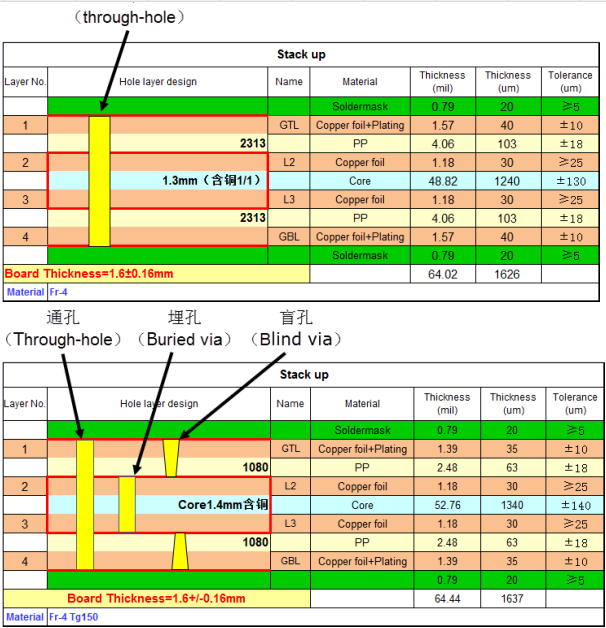
Sequential Lamination PCB for Medical Implants: Building Layer by Layer
Another key technique in HDI PCB manufacturing is sequential lamination. This process involves building the PCB layer by layer, adding insulation and conductive materials step by step to create a multi-layered structure. Each layer is laminated and tested before the next is added, ensuring precision and reliability.
In the context of sequential lamination PCB for medical implants, this method is invaluable. Pacemakers often require 6 to 10 layers or more to accommodate various functions like sensing, pacing, and data transmission. Sequential lamination allows for the creation of these complex boards with high accuracy, reducing the risk of defects that could compromise the device’s performance.
This process also supports the integration of blind and buried vias, which are hidden within the layers of the PCB. These vias save surface space and improve signal routing, making the board more efficient. For pacemakers, where every millimeter counts, sequential lamination ensures that the final product is both compact and robust.
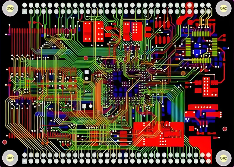
Advanced Routing Techniques for HDI PCBs: Optimizing Signal Paths
Routing refers to the arrangement of conductive paths on a PCB that connect components and carry signals. In HDI PCBs, advanced routing techniques for HDI PCBs are used to manage the high density of connections without sacrificing performance. These techniques include finer trace widths (as small as 0.075 mm), differential pair routing for noise reduction, and controlled impedance paths for consistent signal quality.
For pacemakers, advanced routing is essential to ensure that electrical signals are delivered to the heart with precision. Any delay or distortion in these signals could disrupt the device’s ability to regulate heartbeats. By using HDI-specific routing methods, designers can achieve signal speeds that support real-time monitoring and response, often exceeding 1 GHz in modern designs.
Moreover, advanced routing minimizes electromagnetic interference (EMI), which is critical in a medical setting where other electronic devices might be present. This ensures that the pacemaker operates without interruption, even in challenging environments like hospitals with multiple electronic systems.
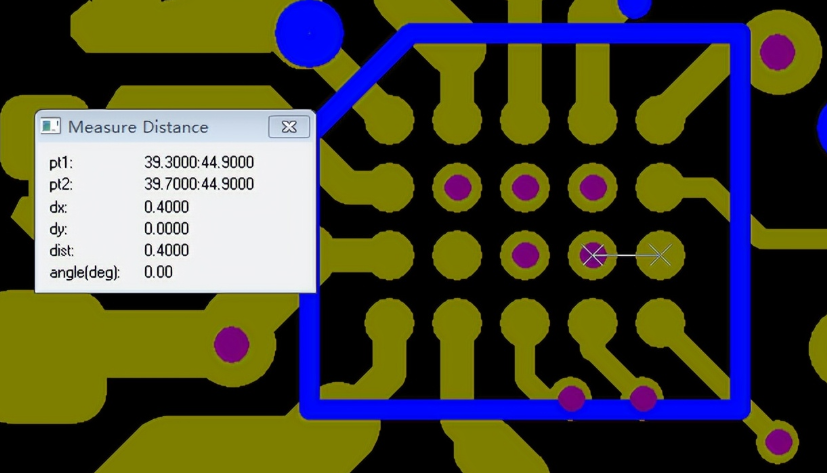
Via-in-Pad Technology for Pacemakers: Maximizing Space Efficiency
Via-in-pad technology is a specialized feature of HDI PCBs where vias are placed directly under component pads rather than beside them. This saves valuable surface space on the board, allowing for even greater component density. In traditional designs, vias require extra space around pads, which limits how closely components can be placed.
When it comes to via-in-pad technology for pacemakers, this innovation is a perfect fit. Pacemakers need to house multiple components—such as microcontrollers, sensors, and capacitors—in an extremely small area. Via-in-pad technology allows designers to place these components closer together, reducing the overall size of the PCB without compromising functionality.
This method also improves electrical performance by shortening the distance signals need to travel, reducing resistance and inductance. For pacemakers, where every microsecond counts in delivering a pulse to the heart, this can make a significant difference. Typical reductions in signal delay can be as much as 10-15% compared to conventional via placement.
Challenges and Considerations in HDI PCB Design for Pacemakers
While HDI PCBs offer numerous benefits, their design and manufacturing come with unique challenges. The complexity of multi-layered boards and microvias requires advanced equipment and skilled technicians, which can increase production costs. Additionally, the strict standards for medical devices mean that every board must undergo rigorous testing to ensure reliability—often involving 100% inspection rates for critical components.
Thermal management is another concern. As components are packed closer together, heat dissipation becomes more difficult. Designers must carefully balance density with cooling solutions to prevent overheating, which could damage the pacemaker or harm the patient. Solutions often include the use of thermal vias and high-conductivity materials to manage temperatures effectively.
Finally, biocompatibility must be considered. Materials used in HDI PCBs for pacemakers must be safe for long-term implantation in the human body, avoiding any risk of toxicity or allergic reactions. This often requires specialized coatings and materials that meet stringent medical regulations.
Future Trends: HDI PCBs in Next-Generation Pacemakers
The future of HDI PCB technology in pacemakers looks promising, with ongoing advancements poised to further improve these devices. One emerging trend is the integration of flexible HDI PCBs, which can conform to the shape of the body for even less invasive implants. These flexible boards maintain the high density of traditional HDI designs while adding a new level of adaptability.
Another area of development is the use of bioresorbable materials in PCB manufacturing. Research is underway to create pacemakers that can dissolve harmlessly in the body after their useful life, eliminating the need for surgical removal. While still in early stages, this technology could revolutionize medical implants in the coming decades.
Lastly, the rise of wireless and IoT-enabled pacemakers will continue to drive demand for HDI PCBs. These devices require complex circuits to support data transmission and remote monitoring, pushing the boundaries of what HDI technology can achieve in terms of density and performance.
Conclusion: The Vital Role of HDI PCBs in Pacemaker Technology
High-Density Interconnect (HDI) PCB technology has transformed the design and functionality of pacemakers, making them smaller, more reliable, and packed with advanced features. From the space-saving power of microvias in pacemaker designs to the precision of sequential lamination PCB for medical implants, every aspect of HDI technology contributes to better patient outcomes. Techniques like advanced routing techniques for HDI PCBs and via-in-pad technology for pacemakers further enhance performance, ensuring that these life-saving devices operate with unmatched accuracy.
As medical technology continues to evolve, HDI PCBs will remain at the forefront, enabling the next generation of pacemakers to be even more innovative and effective. For engineers and designers in the medical field, understanding and leveraging the HDI PCB benefits for pacemakers is essential to creating devices that save lives and improve quality of life.
At ALLPCB, we are committed to supporting the development of cutting-edge medical electronics with high-quality HDI PCB solutions. Whether you’re working on pacemakers or other critical implants, our expertise and advanced manufacturing capabilities can help bring your designs to life with precision and reliability.