 ALLPCB


Selecting the right materials for IoT (Internet of Things) PCBs is critical to ensuring performance, reliability, and cost-effectiveness in your designs. Whether you're working on smart home devices, wearable tech, or industrial sensors, the substrate you choose can make or break your project. In this comprehensive guide, we’ll walk you through the essentials of IoT PCB substrate selection, dive into high frequency PCB materials, explore thermal conductivity in PCBs, and discuss flexible PCB materials for IoT applications. By the end, you’ll have a clear understanding of PCB material properties and how to pick the best option for your needs.
Why IoT PCB Substrate Selection Matters
The substrate is the foundation of any printed circuit board (PCB). It acts as an insulating layer between conductive traces and provides mechanical support. For IoT devices, which often operate in diverse environments and handle complex tasks like wireless communication, the substrate directly impacts signal integrity, thermal management, and durability. Choosing the wrong material can lead to signal loss, overheating, or even device failure. Let’s explore how to make the right choice by breaking down key considerations and material options.

Key Factors in IoT PCB Substrate Selection
When selecting a substrate for IoT applications, several factors come into play. These devices often require a balance of performance, cost, and adaptability to unique design constraints. Below are the most important considerations:
1. Signal Integrity for High Frequency Applications
Many IoT devices rely on wireless communication protocols like Wi-Fi, Bluetooth, or 5G, which operate at high frequencies (often above 1 GHz). At these frequencies, signal integrity becomes a major concern. The substrate’s dielectric constant (Dk) and loss tangent (Df) are critical properties to evaluate. A lower Dk (typically between 2.2 and 4.5) ensures faster signal propagation, while a low Df (below 0.005) minimizes signal loss. For example, materials with a Dk of around 3.0 are often ideal for high-frequency designs, as they reduce crosstalk and maintain signal clarity over long traces.
High frequency PCB materials like PTFE (Polytetrafluoroethylene) or specialized laminates with low dielectric loss are often preferred for such applications. These materials ensure that your IoT device maintains reliable connectivity, even in crowded frequency bands.
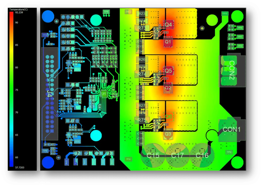
2. Thermal Conductivity for Heat Management
IoT devices are often compact, with components packed tightly together. This can lead to heat buildup, especially in devices with high processing power or continuous operation, like smart sensors or gateways. A substrate with good thermal conductivity in PCBs helps dissipate heat effectively, preventing damage to components and ensuring long-term reliability.
For instance, standard FR-4 substrates have a thermal conductivity of about 0.3 W/m·K, which is sufficient for low-power IoT devices. However, for high-power applications, materials like aluminum-backed substrates or ceramics (with thermal conductivity up to 30 W/m·K) are better choices. These materials can handle temperatures exceeding 150°C without degrading, making them ideal for industrial IoT environments.
3. Mechanical Strength and Flexibility
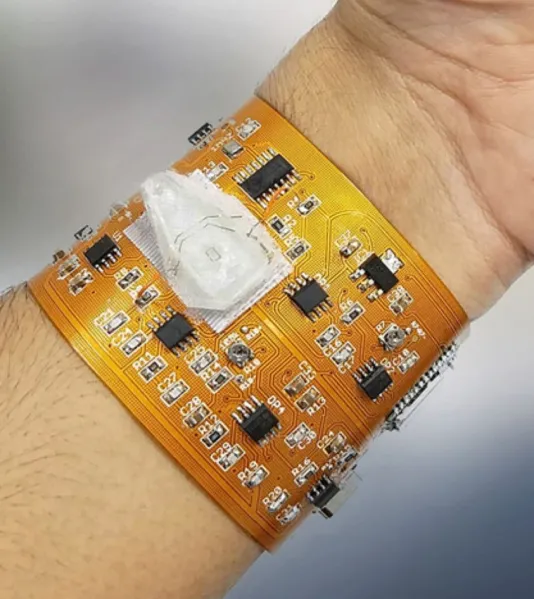
IoT devices come in all shapes and sizes, from rigid industrial controllers to flexible wearables. The substrate must match the mechanical requirements of the application. For rigid boards, materials like FR-4 offer excellent strength and durability. However, for wearables or devices with curved designs, flexible PCB materials for IoT like polyimide (PI) are essential. Polyimide can withstand bending without cracking and operates reliably in temperatures ranging from -40°C to 200°C.
Flexible substrates also reduce the need for connectors, saving space and improving reliability in compact IoT designs. Their lightweight nature is an added bonus for portable devices.
4. Cost and Manufacturability
Cost is always a factor, especially for mass-produced IoT devices. While advanced materials like ceramics or high-end laminates offer superior performance, they can be expensive. FR-4, a widely used epoxy-based material, strikes a good balance between cost and performance for many IoT applications. It’s easy to manufacture, widely available, and supports multi-layer designs, making it a go-to choice for prototypes and consumer-grade devices.
For high-performance needs, you might consider hybrid substrates that combine low-cost materials with specialized layers for specific functions, such as high-frequency signal handling.
Understanding PCB Material Properties for IoT
To make an informed decision, it’s important to understand the core PCB material properties that affect IoT device performance. Here’s a breakdown of the most relevant characteristics:
- Dielectric Constant (Dk): Determines how much a material affects the speed of electrical signals. Lower Dk values (e.g., 2.2-3.5) are better for high-speed and high-frequency designs.
- Loss Tangent (Df): Measures signal loss as it travels through the substrate. A Df below 0.005 is ideal for minimizing energy loss in IoT wireless modules.
- Thermal Conductivity: Indicates how well a material conducts heat. Values above 1 W/m·K are preferable for heat-intensive applications.
- Coefficient of Thermal Expansion (CTE): Reflects how much a material expands or contracts with temperature changes. A lower CTE (closer to that of copper, around 17 ppm/°C) reduces stress on solder joints during thermal cycling.
- Moisture Absorption: High moisture absorption can degrade performance, especially in humid environments. Materials with absorption rates below 0.2% are ideal for outdoor IoT devices.
By matching these properties to your design requirements, you can avoid common issues like signal degradation, overheating, or mechanical failure.
Popular Substrate Materials for IoT PCBs
Now that we’ve covered the key factors and properties, let’s look at some common substrate materials used in IoT PCB design. Each material has its strengths and ideal use cases.
1. FR-4: The Standard Choice
FR-4 is a glass-reinforced epoxy laminate and the most widely used substrate for PCBs. It offers a good balance of cost, mechanical strength, and electrical performance, with a Dk of around 4.5 and a thermal conductivity of 0.3 W/m·K. It’s suitable for most consumer IoT devices, such as smart home gadgets or basic sensors, but may not be ideal for high-frequency or high-temperature applications due to its higher signal loss and limited heat dissipation.
2. PTFE-Based Materials: High Frequency Champions
For IoT devices operating at high frequencies, PTFE-based substrates (often blended with ceramics or glass) are a top choice. They have a low Dk (around 2.2-3.0) and an extremely low Df (below 0.002), ensuring minimal signal loss. These high frequency PCB materials are commonly used in RF modules for IoT devices like smart meters or 5G-enabled sensors. However, they are more expensive and harder to process than FR-4.
3. Polyimide: Flexibility for Wearables
Polyimide is the go-to material for flexible PCB materials in IoT applications. It offers excellent thermal stability (up to 200°C) and can bend without breaking, making it perfect for wearables, medical IoT devices, and compact designs. Its moderate Dk (around 3.5) also supports moderate-frequency signals, though it’s not ideal for ultra-high-frequency needs.
4. Aluminum and Ceramic Substrates: Thermal Powerhouses
For IoT applications requiring high thermal conductivity in PCBs, aluminum-backed substrates and ceramics are excellent options. Aluminum substrates offer thermal conductivity up to 2 W/m·K, while ceramics can reach 30 W/m·K or higher. These materials are ideal for industrial IoT devices or LED-based smart lighting systems that generate significant heat. Their downside is higher cost and limited flexibility.
Special Considerations for IoT Applications
IoT devices often face unique challenges based on their deployment environment and functionality. Here are some additional tips for selecting substrates in specific scenarios:
Outdoor and Harsh Environments
For IoT devices used in outdoor settings, such as agricultural sensors or weather monitors, choose substrates with low moisture absorption and high resistance to temperature fluctuations. Materials like PTFE or specialized FR-4 variants with enhanced environmental resistance can withstand humidity levels up to 90% and temperature swings from -40°C to 85°C.
Miniaturization and Multi-Layer Designs
Many IoT devices require compact, multi-layer PCBs to fit complex circuitry into small spaces. Substrates with high dimensional stability and low CTE are essential to prevent warping during manufacturing. FR-4 and high-Tg (glass transition temperature) materials are often used for multi-layer IoT PCBs due to their reliability under thermal stress.
Power Efficiency for Battery-Powered Devices
Battery-powered IoT devices, like remote sensors, need substrates that minimize power loss. Low-loss materials with a Df below 0.003 help reduce energy consumption in signal transmission, extending battery life. Additionally, lightweight substrates like polyimide can reduce the overall weight of portable devices.
How to Choose the Right Substrate for Your IoT Project
Selecting the best substrate for your IoT PCB involves balancing performance needs with budget constraints. Follow these steps to make an informed decision:
- Define Your Requirements: Identify the operating frequency, thermal load, mechanical constraints, and environmental conditions of your IoT device.
- Match Material Properties: Compare the Dk, Df, thermal conductivity, and CTE of available substrates to your design needs.
- Consider Manufacturing: Ensure the material is compatible with your fabrication processes and available in the required thickness (e.g., 0.8mm to 1.6mm for standard PCBs).
- Evaluate Cost: Weigh the benefits of advanced materials against their price, especially for high-volume production.
- Test and Iterate: Prototype with different substrates if possible to validate performance before finalizing your choice.
Suggested Image Placement: Include a flowchart graphic showing the steps for selecting a PCB substrate. ALT Text: "Flowchart for IoT PCB substrate selection process"
Future Trends in IoT PCB Materials
As IoT technology evolves, so do the materials used in PCB design. Emerging trends include the development of eco-friendly substrates made from bio-based resins, which reduce environmental impact without sacrificing performance. Additionally, advancements in nanotechnology are leading to substrates with even lower dielectric losses and higher thermal conductivity, ideal for next-generation 5G and 6G IoT devices.
Another exciting area is the rise of hybrid substrates, which combine different materials in a single board to optimize performance for specific functions. For example, a board might use a low-loss material for high-frequency traces and a high-thermal-conductivity layer for power components, offering the best of both worlds.
Conclusion: Building Reliable IoT Devices with the Right Materials
Choosing the right substrate is a foundational step in designing IoT PCBs that deliver top performance and reliability. By understanding the nuances of IoT PCB substrate selection, leveraging high frequency PCB materials, prioritizing thermal conductivity in PCBs, and exploring flexible PCB materials for IoT, you can create devices that meet the demands of modern applications. Keep the key PCB material properties in mind—dielectric constant, loss tangent, thermal conductivity, and more—to ensure your design excels in its intended environment.


