ALLPCB


For PCB engineers, understanding the relationship between dielectric thickness and impedance is critical to designing high-performance printed circuit boards. In simple terms, dielectric thickness directly impacts the characteristic impedance of a PCB trace, affecting signal integrity and performance in high-speed circuits. As dielectric thickness increases, impedance typically rises, while a thinner dielectric lowers impedance. This handbook dives deep into this relationship, offering practical insights on PCB impedance calculation, microstrip impedance, stripline impedance, and controlled impedance PCB design. Whether you're working on high-frequency applications or standard designs, mastering these concepts will elevate your engineering skills.
Introduction to Dielectric Thickness and Impedance in PCB Design
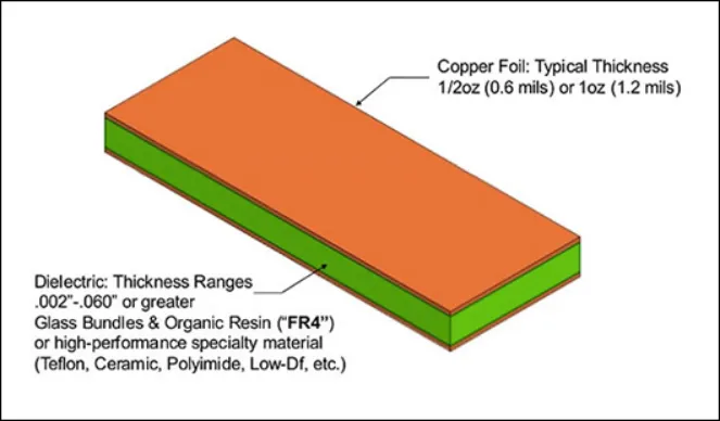
Printed circuit boards (PCBs) are the backbone of modern electronics, and their performance hinges on precise design considerations. One of the most important factors is the relationship between dielectric thickness and impedance. Dielectric thickness refers to the distance between conductive layers, usually filled with an insulating material like FR-4, which has a specific dielectric constant (often around 4.2 to 4.5 at 1 MHz). Impedance, measured in ohms, determines how a signal travels through a trace, impacting signal speed and quality.
In high-speed digital and RF applications, controlling impedance is essential to prevent signal reflections and losses. A mismatch in impedance can lead to data errors or degraded performance. This guide is crafted for PCB engineers who want to understand how dielectric thickness influences impedance and how to apply this knowledge in practical design scenarios. We'll explore key concepts, calculation methods, and guidelines to help you achieve optimal results.
Recommended Reading: Dielectric Thickness in Multilayer PCBs: Optimizing Stackup for Performance
Understanding the Dielectric Thickness and Impedance Relationship
The dielectric thickness and impedance relationship is fundamental to PCB design. Impedance is influenced by several factors, including the width of the trace, the dielectric constant of the material, and the thickness of the dielectric layer. Here's the basic principle: a thicker dielectric layer increases the characteristic impedance of a trace, while a thinner layer decreases it. This happens because the dielectric thickness affects the electric field distribution between the trace and the ground plane.
For instance, in a typical microstrip configuration (where the trace is on the surface of the PCB with a ground plane below), increasing the dielectric thickness from 0.2 mm to 0.4 mm might raise the impedance from 50 ohms to around 65 ohms, assuming other factors like trace width (e.g., 0.3 mm) and dielectric constant (e.g., 4.3) remain constant. This relationship holds true because a thicker dielectric reduces the capacitance per unit length between the trace and ground, leading to higher impedance.
In contrast, a thinner dielectric increases capacitance, lowering impedance. Engineers must balance these factors to match the desired impedance, often 50 ohms for RF applications or 100 ohms for differential pairs in high-speed digital circuits. Understanding this interplay is the first step to designing PCBs with reliable signal integrity.
What is Controlled Impedance in PCB Design?
Controlled impedance refers to the practice of designing PCB traces to have a specific characteristic impedance, ensuring consistent signal transmission. This is crucial for high-speed circuits where signals must travel without distortion or reflection. Controlled impedance PCBs are used in applications like USB, HDMI, Ethernet, and RF systems, where even small deviations in impedance can cause significant performance issues.
To achieve controlled impedance, engineers must carefully select materials, define trace dimensions, and control dielectric thickness. For example, a common target impedance for single-ended traces in high-speed designs is 50 ohms. Achieving this requires precise calculations and often the use of specialized manufacturing processes to maintain tight tolerances on dielectric thickness and trace geometry.
Microstrip Impedance: Key Factors and Calculations
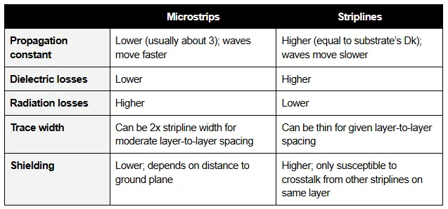
Microstrip is a common PCB trace configuration where the conductor is on the outer layer of the board, separated from a ground plane by a dielectric layer. Microstrip impedance depends on trace width, dielectric thickness, and the dielectric constant of the material. The relationship can be approximated using standard formulas or online calculators tailored for PCB design.
A widely used formula for microstrip impedance (Z?) is:
Z? = (87 / √(εr + 1.41)) * ln(5.98 * H / (0.8 * W + T))
Where:
- Z? is the characteristic impedance in ohms
- εr is the dielectric constant of the material (e.g., 4.3 for FR-4)
- H is the dielectric thickness in mils (e.g., 8 mils)
- W is the trace width in mils (e.g., 6 mils)
- T is the trace thickness in mils (e.g., 1.4 mils for 1 oz copper)
For example, with a dielectric thickness of 8 mils, trace width of 6 mils, trace thickness of 1.4 mils, and dielectric constant of 4.3, the impedance might calculate to approximately 50 ohms, a common target for many designs. Adjusting the dielectric thickness to 10 mils would increase the impedance to around 55 ohms, illustrating the direct relationship.
Engineers often use simulation software or online tools to refine these calculations, ensuring accuracy for specific board materials and stackups. Testing and validation during prototyping are also critical to confirm that the calculated impedance matches the actual performance.
Stripline Impedance: How It Differs from Microstrip
Unlike microstrip, stripline involves a trace embedded between two ground planes, fully surrounded by dielectric material. This configuration offers better shielding from external interference, making it ideal for high-frequency applications. However, stripline impedance calculations are more complex due to the dual dielectric layers above and below the trace.
The formula for stripline impedance (Z?) can be approximated as:
Z? = (60 / √εr) * ln(1.9 * B / (0.8 * W + T))
Where:
- Z? is the characteristic impedance in ohms
- εr is the dielectric constant
- B is the total dielectric thickness between the two ground planes in mils
- W is the trace width in mils
- T is the trace thickness in mils
For instance, with a total dielectric thickness (B) of 20 mils, trace width of 5 mils, trace thickness of 1.4 mils, and dielectric constant of 4.3, the impedance might be around 50 ohms. Increasing B to 25 mils could raise the impedance to approximately 53 ohms, again showing how dielectric thickness impacts impedance.
Stripline typically has lower impedance than microstrip for the same dielectric thickness due to the increased capacitance from having ground planes on both sides. This makes it a preferred choice for applications requiring tight impedance control and minimal signal interference.
Practical Guidelines for PCB Impedance Calculation
Calculating PCB impedance accurately is essential for achieving controlled impedance designs. Here are practical steps and tips to guide you through the process:
- Determine Target Impedance: Identify the required impedance for your application, such as 50 ohms for single-ended RF signals or 100 ohms for differential pairs in high-speed digital circuits.
- Select Materials: Choose a dielectric material with a known dielectric constant. For standard designs, FR-4 with a dielectric constant of 4.2 to 4.5 is common. For high-frequency designs, consider materials like Rogers with lower dielectric constants (e.g., 3.0 to 3.5).
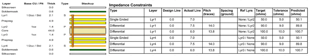
- Define Stackup: Work with your PCB manufacturer to define the layer stackup, including dielectric thicknesses between layers. Ensure the stackup supports your target impedance.
- Use Calculation Tools: Leverage online calculators or simulation software to input parameters like trace width, dielectric thickness, and dielectric constant. These tools provide quick estimates for microstrip and stripline configurations.
- Validate with Testing: After manufacturing, use a Time Domain Reflectometer (TDR) to measure actual impedance and compare it with your calculations. Adjust trace widths or dielectric thicknesses if necessary during redesign.
Keep in mind that manufacturing tolerances can affect impedance. For instance, a variation of ±10% in dielectric thickness can shift impedance by a few ohms, potentially causing signal integrity issues in critical applications. Always specify tight tolerances for controlled impedance designs and collaborate closely with your PCB fabricator.
Design Tips for Controlled Impedance PCBs
Designing a controlled impedance PCB requires attention to detail and adherence to best practices. Here are actionable tips to ensure success:
- Maintain Consistent Dielectric Thickness: Variations in dielectric thickness across the board can lead to impedance mismatches. Specify uniform thickness in your stackup design.
- Optimize Trace Geometry: Adjust trace width and spacing to achieve the target impedance. Wider traces lower impedance, while narrower traces increase it.
- Minimize Vias: Vias introduce impedance discontinuities. Use them sparingly in high-speed signal paths and consider back-drilling for critical designs to reduce stub effects.
- Choose Appropriate Materials: High-frequency designs benefit from low-loss dielectrics with stable dielectric constants over a wide frequency range.
- Simulate Before Manufacturing: Use electromagnetic simulation tools to model your design and predict impedance behavior under real-world conditions.
By following these guidelines, you can reduce the risk of signal integrity issues and ensure your PCB performs as intended in its final application.
Common Challenges in Managing Dielectric Thickness and Impedance
Even with careful planning, engineers often face challenges when dealing with dielectric thickness and impedance. Here are some common issues and how to address them:
- Material Variations: Dielectric constants can vary between batches of material, affecting impedance. Work with suppliers to ensure consistent material properties or account for variations in your design margins.
- Manufacturing Tolerances: Small deviations in dielectric thickness or trace etching during production can alter impedance. Specify tight tolerances (e.g., ±5% for dielectric thickness) and request impedance testing reports from your manufacturer.
- High-Frequency Effects: At higher frequencies, skin effect and dielectric losses become significant, altering effective impedance. Use low-loss materials and wider traces for high-frequency designs to mitigate these effects.
Addressing these challenges early in the design phase can save time and cost during PCB prototyping and production.
Conclusion: Mastering Dielectric Thickness and Impedance for Better PCBs
The relationship between dielectric thickness and impedance is a cornerstone of effective PCB design. By understanding how dielectric thickness influences impedance in microstrip and stripline configurations, engineers can make informed decisions to optimize signal integrity and performance. Whether you're calculating PCB impedance for a high-speed digital circuit or designing a controlled impedance PCB for RF applications, the principles and guidelines in this handbook provide a solid foundation.
Start by mastering the basics of impedance calculation and applying best practices for controlled impedance designs. Use simulation tools, collaborate with your PCB manufacturer, and validate your designs through testing. With these strategies, you'll be well-equipped to tackle the complexities of modern PCB engineering and deliver reliable, high-quality boards for any application.