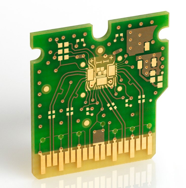
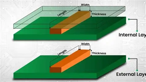
If you're delving into printed circuit board (PCB) design, you might have come across the term "PCB aspect ratio" and wondered what it means and why it matters. Simply put, the PCB aspect ratio is the ratio of the board's thickness to the diameter of the smallest drilled hole (via). It plays a critical role in ensuring the reliability and manufacturability of your PCB. In this comprehensive guide, we'll break down the PCB aspect ratio definition, explain PCB aspect ratio calculation, explore the optimal PCB aspect ratio for designs, discuss the PCB thickness to hole diameter ratio, and highlight the PCB aspect ratio importance in creating high-quality boards. Whether you're a beginner or a seasoned engineer, this guide will equip you with the knowledge to optimize your designs.
What Is PCB Aspect Ratio? A Clear Definition
The PCB aspect ratio refers to the relationship between the thickness of a PCB and the diameter of the smallest hole drilled through it, typically a via. Vias are tiny holes that allow electrical connections between different layers of a multi-layer PCB. The aspect ratio is expressed as a numerical value, such as 8:1, where the first number represents the board thickness, and the second represents the hole diameter. For example, if a PCB is 1.6mm thick and the smallest via diameter is 0.2mm, the aspect ratio is 8:1.
This ratio is a crucial parameter in PCB manufacturing because it directly impacts the ability to plate copper inside the via effectively. A higher aspect ratio means a thicker board relative to a smaller hole, which can pose challenges during the plating process. Understanding this definition is the first step to mastering PCB design for reliability and performance.
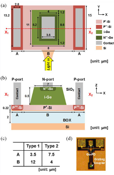
Why Is PCB Aspect Ratio Important?
The PCB aspect ratio importance cannot be overstated in the world of electronics design. This metric affects multiple aspects of PCB manufacturing and performance, including:
- Manufacturability: During the plating process, copper must be deposited uniformly inside the vias to ensure reliable electrical connections. A high aspect ratio (e.g., 10:1 or above) can make it difficult for plating solutions to flow through the narrow holes, leading to uneven copper deposition or voids. This can result in weak connections or complete failures.
- Reliability: Vias with poor plating are prone to cracking or breaking under thermal stress or mechanical strain, especially in high-temperature applications. A balanced aspect ratio helps maintain structural integrity.
- Signal Integrity: For high-speed designs, vias with improper aspect ratios can introduce impedance mismatches, leading to signal loss or interference. A well-designed aspect ratio ensures consistent electrical performance.
- Cost Efficiency: Pushing the limits of aspect ratio (e.g., extremely small vias in thick boards) often requires advanced manufacturing techniques, which can increase production costs. Staying within recommended ratios helps keep expenses in check.
By paying attention to the aspect ratio, designers can avoid common pitfalls and create boards that are both functional and cost-effective.
How to Calculate PCB Aspect Ratio: A Step-by-Step Guide
Understanding PCB aspect ratio calculation is straightforward and essential for any designer. Here's how to do it:
- Determine the PCB Thickness: Measure the total thickness of your PCB, including all layers and prepreg materials. For a standard four-layer board, this might be 1.6mm, a common industry standard.
- Identify the Smallest Hole Diameter: Find the diameter of the smallest drilled hole on your board. This is typically the via used for interlayer connections. For example, this might be 0.3mm.
- Divide Thickness by Diameter: Perform the division to get the aspect ratio. Using the numbers above, 1.6mm ÷ 0.3mm = 5.33. Thus, the aspect ratio is approximately 5.3:1.
This calculation helps you assess whether your design falls within acceptable manufacturing limits. Most standard fabrication processes can handle aspect ratios up to 8:1 or 10:1 without issues. Beyond that, you may need specialized techniques or risk manufacturing defects.
What Is the Optimal PCB Aspect Ratio for Designs?
Finding the optimal PCB aspect ratio depends on your specific project requirements, including board complexity, layer count, and application. However, there are general guidelines that most designers follow to balance performance and manufacturability:
- Standard Designs: For most consumer electronics and general-purpose PCBs, an aspect ratio between 6:1 and 8:1 is considered optimal. For a 1.6mm thick board, this translates to via diameters of approximately 0.2mm to 0.27mm. This range ensures reliable plating and keeps costs low.
- High-Density Designs: In applications requiring high-density interconnects (HDI), such as smartphones or advanced medical devices, aspect ratios may push toward 10:1. These designs often use microvias with diameters as small as 0.1mm on thinner boards (e.g., 1mm thick). However, this requires advanced manufacturing capabilities.
- Thick Boards or Power Applications: For thicker boards used in power electronics (e.g., 2.4mm or more), maintaining a lower aspect ratio (around 5:1) is often necessary. This means using larger via diameters (e.g., 0.5mm) to ensure proper plating and thermal management.
Choosing the right ratio involves balancing the need for compact design with the practical limits of fabrication. Always consult with your manufacturing partner to confirm their capabilities before finalizing your design.
Understanding PCB Thickness to Hole Diameter Ratio
The PCB thickness to hole diameter ratio is essentially another way of describing the aspect ratio. It emphasizes the relationship between these two critical dimensions and their impact on design success. A few key considerations include:
- Impact on Drilling: Smaller holes in thicker boards (high ratios) are harder to drill accurately. This can lead to misalignment or breakage of drill bits, increasing defect rates.
- Plating Challenges: As mentioned earlier, a high thickness-to-diameter ratio complicates the electroplating process. For instance, a 2mm thick board with 0.2mm vias (10:1 ratio) may suffer from insufficient copper deposition at the center of the via, weakening the connection.
- Thermal and Mechanical Stress: Vias with extreme ratios are more susceptible to stress during thermal cycling (e.g., temperature changes from -40°C to 85°C in automotive applications). This can cause cracks or delamination, reducing the board's lifespan.
To mitigate these issues, designers often adjust board thickness or via size. For example, reducing a board's thickness from 2mm to 1.6mm while keeping a 0.2mm via lowers the ratio from 10:1 to 8:1, improving manufacturability.
Practical Tips for Optimizing PCB Aspect Ratio in Your Designs
Now that we've covered the basics, let's dive into actionable strategies to optimize the aspect ratio for your PCB designs. These tips will help you achieve reliable, cost-effective results:
1. Start with Standard Specifications
Begin with industry-standard board thicknesses like 1.6mm for most designs. Pair this with via diameters of 0.3mm or larger to maintain an aspect ratio below 6:1. This approach works well for a wide range of applications and minimizes manufacturing risks.
2. Consider Layer Count Early
The number of layers in your PCB directly affects its thickness. A six-layer board might be 2mm thick, while a two-layer board could be as thin as 0.8mm. Plan your layer count early to avoid ending up with an unmanageable aspect ratio when selecting via sizes.
3. Use Larger Vias When Possible
If your design allows, opt for slightly larger via diameters (e.g., 0.4mm instead of 0.2mm). This reduces the aspect ratio and improves plating reliability, especially on thicker boards. Larger vias also enhance thermal dissipation in power-heavy designs.
4. Leverage Advanced Technologies for HDI
For high-density designs requiring tiny vias (e.g., 0.1mm), consider using technologies like laser drilling for microvias. These methods are better suited for high aspect ratios (10:1 or more) and ensure precision in compact layouts.
5. Test and Validate with Prototypes
Before mass production, create prototypes to test your aspect ratio under real-world conditions. For instance, if your design has an 8:1 ratio, subject the prototype to thermal cycling and mechanical stress tests to confirm via integrity.

Common Pitfalls to Avoid with PCB Aspect Ratio
Even experienced designers can make mistakes when dealing with aspect ratios. Here are some common issues to watch out for:
- Ignoring Manufacturer Limits: Every fabrication house has specific limits on aspect ratios, often between 8:1 and 12:1 for standard processes. Exceeding these limits without prior consultation can lead to rejected designs or costly rework.
- Over-Optimizing for Size: Shrinking via sizes to fit more components on a board might seem like a good idea, but it can push the aspect ratio too high, compromising reliability. Balance compactness with practicality.
- Neglecting Signal Requirements: High-speed signals (e.g., operating at 5 GHz) require controlled impedance, which can be disrupted by poorly designed vias. Ensure your aspect ratio supports the electrical characteristics needed for your application.
How Aspect Ratio Impacts Different PCB Applications
The importance of aspect ratio varies depending on the end-use of the PCB. Let's explore how it affects different applications:
- Consumer Electronics: Devices like smartphones and laptops often use HDI PCBs with aspect ratios of 8:1 to 10:1 to accommodate dense layouts. Reliability is critical, as failures can lead to costly recalls.
- Automotive Systems: PCBs in vehicles must withstand harsh conditions, including temperature swings and vibrations. A moderate aspect ratio (e.g., 6:1) with larger vias ensures durability over time.
- Industrial Equipment: Thick boards with low aspect ratios (e.g., 5:1) are common in industrial applications where power handling and thermal management take precedence over compactness.
- Medical Devices: Precision and reliability are paramount in medical electronics. Designers often target moderate ratios (6:1 to 8:1) to ensure consistent performance in life-critical systems.
Understanding your application's specific needs will guide you in selecting the right aspect ratio for optimal results.
Conclusion: Mastering PCB Aspect Ratio for Better Designs
The journey to creating high-performing PCBs starts with understanding and optimizing the PCB aspect ratio. From grasping the basic PCB aspect ratio definition to mastering PCB aspect ratio calculation, and from determining the optimal PCB aspect ratio to appreciating the PCB thickness to hole diameter ratio, every step is vital. The PCB aspect ratio importance lies in its direct impact on manufacturability, reliability, and cost-efficiency of your designs.
By following the guidelines and tips outlined in this guide, you can avoid common pitfalls, balance design constraints, and create PCBs that meet both technical and practical requirements. Whether you're working on consumer gadgets, automotive systems, or medical devices, a well-considered aspect ratio is the foundation of a successful design. Partner with a trusted manufacturing service to bring your optimized designs to life with precision and quality.

 ALLPCB


