 ALLPCB


When designing a printed circuit board (PCB), safety is a top priority, especially when dealing with high voltages. One critical factor to consider is creepage distance—the shortest path between two conductive parts measured along the surface of the insulating material. Understanding and calculating creepage distance ensures your PCB design prevents electrical arcing, breakdown, and potential hazards. In this guide, we’ll dive deep into creepage distance, covering topics like PCB creepage distance calculation, creepage distance standards IEC, creepage distance for high voltage PCB, and reinforced insulation creepage distance. Let’s explore how to design safer and more reliable PCBs.
What Is Creepage Distance and Why Does It Matter?
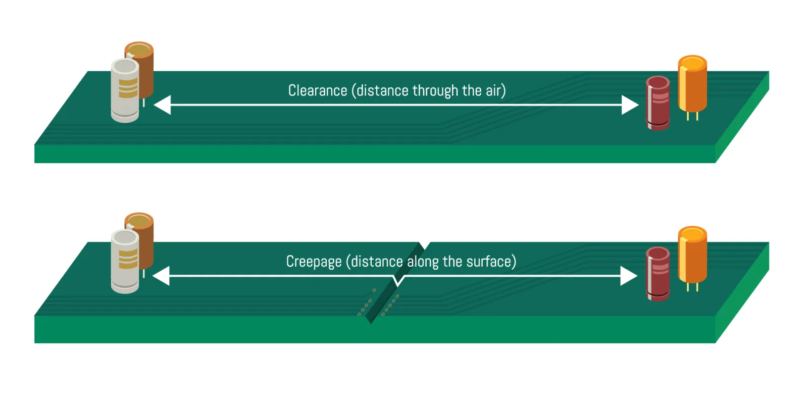
Creepage distance is the surface distance between two conductive elements on a PCB, such as traces, pads, or components. Unlike clearance, which is the shortest distance through air, creepage distance accounts for the path over the insulating material’s surface. This measurement is vital because, over time, factors like dust, moisture, and pollution can reduce the insulating properties of the surface, leading to electrical breakdown or arcing.
In high-voltage applications, insufficient creepage distance can result in catastrophic failures, including fires or equipment damage. By adhering to proper creepage distances, you ensure safety, compliance with international standards, and long-term reliability of your PCB designs. Whether you’re working on consumer electronics, industrial equipment, or medical devices, understanding creepage distance is non-negotiable.
Key Factors Influencing Creepage Distance in PCB Design
Several variables affect the required creepage distance in a PCB layout. Let’s break them down to help you design with precision.
1. Working Voltage
The voltage level across the conductors directly impacts the required creepage distance. Higher voltages increase the risk of arcing, so the creepage distance must be larger. For instance, a PCB operating at 500V will need a significantly greater creepage distance than one operating at 50V. Specific standards provide tables to determine exact distances based on voltage levels, which we’ll discuss later.
2. Pollution Degree
Pollution degree refers to the environmental conditions where the PCB will operate. It’s categorized into levels (1 to 4) based on the likelihood of conductive contaminants like dust or moisture. For example, a PCB in a clean, controlled environment (Pollution Degree 1) requires less creepage distance than one in an industrial setting with heavy dust (Pollution Degree 3).
3. Material Properties (CTI Value)
The Comparative Tracking Index (CTI) of the PCB material measures its resistance to tracking—forming a conductive path due to surface breakdown. Materials with a higher CTI value (like FR-4 with a CTI of 175-250) can have shorter creepage distances compared to materials with lower CTI values. Choosing the right material is critical for high-voltage designs.
4. Altitude
At higher altitudes, air density decreases, reducing its insulating properties. If your PCB will operate above 2000 meters, you may need to increase creepage distances to compensate for the reduced insulation provided by thinner air.
5. Type of Insulation
Creepage distance requirements vary depending on the type of insulation—functional, basic, or reinforced. Reinforced insulation, used in applications requiring higher safety (like medical devices), demands greater creepage distances to provide an extra layer of protection against failure.
Creepage Distance Standards: IEC Guidelines
When designing PCBs, compliance with international standards ensures safety and market acceptance. The International Electrotechnical Commission (IEC) provides widely recognized guidelines for creepage distance. The most relevant standard for PCB design is IEC 60950-1 (now largely replaced by IEC 62368-1 for IT and AV equipment), which outlines creepage and clearance requirements based on voltage, pollution degree, and material group.
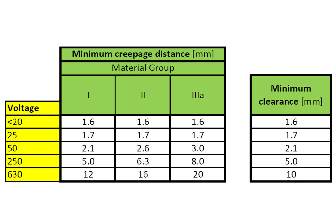
IEC Creepage Distance Tables
IEC standards categorize materials into groups based on their CTI values and provide tables to determine minimum creepage distances. For example, under Pollution Degree 2 (typical for office environments) and a working voltage of 250V RMS, the minimum creepage distance for a Material Group I (CTI ≥ 600) is approximately 2.5mm. For Material Group III (CTI 100-175), this distance increases to around 4mm.
Reinforced Insulation Creepage Distance
For applications requiring reinforced insulation, such as power supplies in medical equipment, the creepage distance must be doubled compared to basic insulation under the same conditions. This ensures an additional safety margin. For instance, if basic insulation requires a 3mm creepage distance at 300V, reinforced insulation would demand at least 6mm.
Adhering to these IEC standards not only ensures safety but also helps your product pass regulatory testing for global markets. Always consult the specific IEC standard relevant to your industry for the most accurate and up-to-date requirements.
PCB Creepage Distance Calculation: A Step-by-Step Guide
Calculating the correct creepage distance for your PCB design involves a systematic approach. Here’s how to do it effectively.
Step 1: Determine the Working Voltage
Identify the maximum voltage (AC or DC) between the conductors. Include any transient overvoltages that might occur during operation. For example, a power supply PCB might have a working voltage of 400V DC with occasional spikes up to 600V.
Step 2: Assess the Environment (Pollution Degree)
Evaluate the operating environment. A cleanroom might be Pollution Degree 1, while an outdoor industrial application could be Pollution Degree 3 or 4. This directly affects the required distance.
Step 3: Check Material Properties
Look up the CTI value of your PCB material to determine its material group under IEC standards. Most standard FR-4 laminates fall into Material Group IIIa or IIIb (CTI 100-175), requiring larger creepage distances.
Step 4: Refer to IEC Tables or Tools
Use the appropriate IEC standard table to find the minimum creepage distance based on voltage, pollution degree, and material group. Alternatively, online calculators tailored to IEC 62368-1 or other standards can simplify this process by inputting your parameters.
Step 5: Adjust for Insulation Type and Altitude
If your design requires reinforced insulation, double the creepage distance. If operating at high altitudes (above 2000m), apply a correction factor as per the standard—often increasing the distance by 1% per 100m above 2000m.
By following these steps, you can ensure your PCB meets safety requirements. For a practical example, a high-voltage PCB operating at 500V in a Pollution Degree 2 environment with FR-4 material (Material Group III) might require a creepage distance of at least 5mm for basic insulation, or 10mm for reinforced insulation.
Creepage Distance for High Voltage PCB Design
High-voltage PCBs, often used in power supplies, electric vehicles, and industrial machinery, face unique challenges. Voltages above 300V significantly increase the risk of arcing and surface breakdown, making creepage distance a critical design parameter.
Design Tips for High Voltage PCBs
- Wider Spacing: Always exceed the minimum creepage distance for high-voltage designs. For a 1000V application under Pollution Degree 2, IEC standards might suggest a creepage distance of 8mm or more, depending on the material.
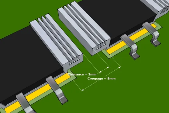
- Slots and Barriers: Adding slots or physical barriers in the PCB can increase the effective creepage distance by forcing the path to go around the slot. This is especially useful in compact designs where space is limited.
- Conformal Coating: Applying a conformal coating can reduce the pollution degree by protecting the PCB surface from contaminants, potentially allowing shorter creepage distances.
- Material Selection: Opt for high-CTI materials (like specialized laminates with CTI > 400) to minimize required creepage distances in high-voltage applications.
High-voltage designs often operate in harsh environments, so combining proper creepage distance with robust materials and protective measures ensures reliability and safety.
Suggested Reading:Creepage and Clearance: The MVPs of High-Voltage PCB Spacing
Practical Applications of Creepage Distance in PCB Design
Understanding creepage distance is essential across various industries. Here are a few examples of how it applies in real-world scenarios.
Consumer Electronics
In devices like power adapters, creepage distance ensures user safety by preventing arcing between high-voltage components and accessible parts. A typical adapter might require a 3mm creepage distance for 230V AC input under basic insulation.
Medical Equipment
Medical devices often require reinforced insulation to protect patients and operators. A defibrillator PCB, for instance, might need a creepage distance of 8mm or more at 500V to meet stringent safety standards.
Industrial Systems
In industrial motor drives operating at 600V or higher, creepage distances of 10mm or more are common to account for pollution and high voltage. Slots and barriers are often used to enhance safety in these designs.
By tailoring creepage distances to the application, you can design PCBs that meet both functional and safety requirements.
Common Mistakes to Avoid in Creepage Distance Design
Even experienced designers can make errors when calculating or implementing creepage distances. Here are some pitfalls to watch out for:
- Underestimating Voltage Spikes: Failing to account for transient voltages can lead to insufficient creepage distances. Always design for the worst-case scenario.
- Ignoring Environmental Factors: Assuming a clean environment (Pollution Degree 1) when the PCB will operate in a harsher setting can compromise safety.
- Overlooking Insulation Type: Not doubling creepage distances for reinforced insulation in critical applications like medical devices can result in non-compliance.
- Poor Layout Practices: Placing high-voltage traces too close to low-voltage areas without barriers or slots can violate creepage requirements.
Double-checking your design against standards and using simulation tools can help catch these issues early.
Tools and Resources for Creepage Distance Calculation
Designing for creepage distance doesn’t have to be a manual process. Several tools and resources can simplify the task:
- Online Calculators: Websites offer free creepage distance calculators based on IEC standards, allowing you to input voltage, pollution degree, and material properties for instant results.
- Design Software: Many a PCB design software include built-in rules for creepage and clearance, automatically flagging violations during layout.
- IEC Standards: Access the latest IEC 62368-1 or other relevant standards for detailed tables and guidelines.
Using these tools ensures accuracy and saves time, especially for complex high-voltage designs.
Conclusion: Prioritizing Safety with Creepage Distance
Creepage distance is a cornerstone of safe PCB design, particularly for high-voltage applications. By understanding factors like working voltage, pollution degree, and material properties, and by adhering to creepage distance standards like those from IEC, you can create designs that prevent electrical failures and ensure user safety. Whether you’re calculating PCB creepage distance for a simple consumer device or a complex industrial system, following the guidelines for reinforced insulation creepage distance and high-voltage PCB design is essential.
Take the time to calculate distances accurately, choose appropriate materials, and incorporate protective features like slots or coatings. With the right approach, your PCB designs will not only meet safety standards but also deliver reliable performance in any environment. Trust in thorough planning and adherence to standards to build safer, better PCBs for every application.


