 ALLPCB


In the fast-evolving world of LED lighting, achieving brighter, more efficient, and reliable systems starts with a well-designed printed circuit board (PCB). High-density LED PCB layout is the backbone of modern lighting solutions, ensuring optimal performance, heat management, and durability. Whether you're designing for commercial lighting, automotive applications, or smart home systems, mastering high-density LED PCB layout, optimizing thermal vias for LED PCBs, and leveraging techniques like micro-via PCB design for LED lighting can make all the difference.
In this comprehensive guide, we'll explore the critical aspects of designing PCBs for high-density LED arrays. From advanced layout strategies to thermal management and high-current handling, you'll gain actionable insights to elevate your LED lighting projects. Let’s dive into the details of creating efficient and powerful LED systems with cutting-edge PCB design techniques.
Why High-Density LED PCB Design Matters
LED lighting has revolutionized energy efficiency and illumination across industries. However, packing multiple LEDs into a compact space—known as high-density LED design—introduces unique challenges. These include heat buildup, current distribution, and signal integrity. A poorly designed PCB can lead to uneven lighting, reduced lifespan, and even system failure.
A well-executed high-density LED PCB layout addresses these issues by optimizing space, ensuring even current flow, and managing heat dissipation. By focusing on advanced design principles, you can boost lumens (light output) while maintaining reliability. Let’s break down the key elements that make high-density LED PCB design so crucial.
Key Principles of High-Density LED PCB Layout
Designing a PCB for high-density LED applications requires careful planning and attention to detail. Here are the core principles to follow for a successful layout:
1. Component Placement for Optimal Performance
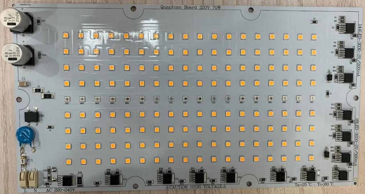
In a high-density LED PCB layout, the placement of LEDs and supporting components is critical. Arrange LEDs to minimize shadowing and ensure uniform light distribution. Place driver circuits and power components close to the LEDs to reduce trace lengths, which helps lower resistance and voltage drops. For instance, a typical high-density design might involve spacing LEDs just 2-3 mm apart, requiring precise placement to avoid interference.
2. Trace Width and Spacing for High-Current Needs
LEDs, especially in high-density arrays, often demand significant current. Traces must be wide enough to handle this without overheating. A general guideline for high-current LED PCB design is to use trace widths of at least 0.5 mm for currents up to 1A, scaling up to 1.5-2 mm for currents between 2-3A. Additionally, maintain adequate spacing (at least 0.2 mm) between traces to prevent crosstalk and short circuits in compact layouts.
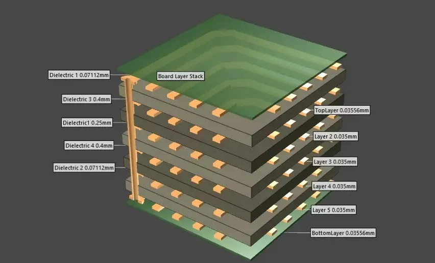
3. Layer Stack-Up for Signal Integrity
For complex LED arrays, consider a multi-layer PCB design. A 4-layer board, for example, can dedicate separate layers for power, ground, and signal routing. This reduces electromagnetic interference (EMI) and ensures stable operation. In advanced LED array PCB design, a ground plane directly beneath the LED layer can also act as a heat sink, aiding PCB thermal management.
Thermal Management: Optimizing Thermal Vias for LED PCBs
Heat is the enemy of LED performance and longevity. High-density designs generate significant heat due to the close proximity of components. Without proper thermal management, LEDs can overheat, leading to color shifts, reduced brightness, and premature failure. Optimizing thermal vias for LED PCBs is one of the most effective ways to manage heat.
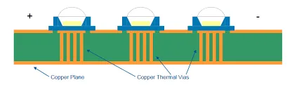
What Are Thermal Vias and Why Do They Matter?
Thermal vias are small holes drilled through the PCB, filled or plated with conductive material like copper, to transfer heat from the LED components to a heat sink or another layer of the board. In high-density LED designs, thermal vias are placed directly under or near the LED pads to create a direct path for heat dissipation.
Best Practices for Thermal Via Design
- Via Size and Count: Use vias with a diameter of 0.3-0.5 mm for effective heat transfer. Place multiple vias (e.g., 4-6 per LED) under high-power LEDs to maximize heat dissipation.
- Via Placement: Position thermal vias as close as possible to the LED thermal pad. Avoid placing them under traces carrying high-frequency signals to prevent interference.
- Copper Fill: Opt for filled or plugged vias to enhance thermal conductivity. A copper-filled via can improve heat transfer by up to 30% compared to an open via.
- Connection to Heat Sink: Ensure thermal vias connect to a large copper plane or external heat sink on the bottom layer for optimal heat spreading.
By following these guidelines, you can significantly lower the junction temperature of LEDs, often by 10-20°C, extending their lifespan and maintaining consistent light output.
Micro-Via PCB Design for LED Lighting: Precision in Compact Spaces
As LED lighting systems become smaller and more powerful, traditional via structures may not fit within the tight constraints of high-density layouts. This is where micro-via PCB design for LED lighting comes into play. Micro-vias are tiny vias, typically less than 0.15 mm in diameter, created using laser drilling for high-precision applications.
Advantages of Micro-Vias in LED PCBs
- Space Efficiency: Microvias allow for denser routing, freeing up space on the PCB surface for more LEDs or components.
- Improved Thermal Paths: Though smaller, micro-vias can still contribute to heat dissipation when used in large numbers or combined with thermal pads.
- Better Signal Integrity: In multi-layer designs, micro-vias reduce signal path lengths, minimizing delays and EMI—crucial for smart LED systems with integrated controls.
Design Tips for Micro-Vias
When incorporating micro-vias, ensure they are stacked or staggered carefully to avoid weakening the board structure. Limit the aspect ratio (depth-to-diameter) to 1:1 for reliable manufacturing. For example, a micro-via with a 0.1 mm diameter should not exceed 0.1 mm in depth. Additionally, work with a manufacturer capable of handling high-density interconnect (HDI) processes to ensure precision.
Advanced LED Array PCB Design: Maximizing Efficiency and Output
For applications requiring intense illumination, such as stadium lighting or industrial systems, advanced LED array PCB design is essential. These designs often involve dozens or hundreds of LEDs working together, demanding careful planning for power delivery, thermal management, and light uniformity.
Grid and Cluster Layouts
Organize LEDs in grid or cluster patterns to balance light distribution and heat generation. A grid layout works well for uniform lighting, while clusters are ideal for focused beams. Use simulation software to predict light output and adjust spacing—typically 5-10 mm for high-power arrays—to avoid hot spots.
Power Distribution Networks
In advanced arrays, uneven current distribution can cause some LEDs to burn brighter (and hotter) than others. Design a robust power distribution network with equal trace lengths to each LED group. For a 100-LED array drawing 10A total, split the current into smaller branches (e.g., 1A per 10 LEDs) to prevent overloading any single path.
High-Current LED PCB Design Guidelines
High-power LEDs often require currents exceeding 1A per unit, making high-current LED PCB design guidelines a priority for safety and performance. Here are key strategies to handle high currents effectively:
1. Use Thicker Copper Layers
Standard PCBs use 1 oz/ft2 copper (about 35 μm thick), which may not suffice for high-current applications. Opt for 2 oz/ft2 or even 3 oz/ft2 copper to reduce resistance and heat buildup. For a 3A current, a 2 oz/ft2 copper trace should be at least 1.5 mm wide to stay within safe temperature limits.
2. Minimize Voltage Drops
Long traces increase resistance, leading to voltage drops that dim LEDs. Keep power traces short and direct, and place decoupling capacitors (e.g., 0.1 μF) near each LED to stabilize voltage. A voltage drop of less than 0.1V per trace segment is ideal for consistent performance.
3. Reinforce with Busbars or Planes
For currents above 5A, consider integrating copper busbars or dedicated power planes. These provide low-resistance paths, reducing heat and ensuring even current distribution across the board.
Material Selection for High-Density LED PCBs
The choice of PCB material impacts thermal performance and durability. For high-density LED applications, consider these options:
- FR-4 with High Tg: Standard FR-4 works for low to medium power LEDs but choose a high glass transition temperature (Tg) variant (e.g., 170°C) for better heat resistance.
- Aluminum Core PCBs: Metal-core PCBs (MCPCBs) with aluminum bases are ideal for high-power LEDs due to their excellent thermal conductivity (1-2 W/m·K compared to 0.3 W/m·K for FR-4).
- Ceramic Substrates: For extreme heat and high reliability, ceramic materials like alumina offer superior thermal performance (up to 30 W/m·K) but at a higher cost.
Selecting the right material can reduce operating temperatures by 15-25°C, significantly enhancing LED lifespan.
Simulation and Testing: Ensuring Design Success
Before manufacturing, use simulation tools to validate your high-density LED PCB design. Thermal simulation can predict hot spots, while current flow analysis ensures even power distribution. Post-production, test the board under full load to measure temperature (aim for below 85°C at the LED junction) and light output consistency.
Conclusion: Lighting the Way with High-Density LED PCB Design
Designing PCBs for high-density LED lighting is both an art and a science. By focusing on high-density LED PCB layout, optimizing thermal vias for LED PCBs, and embracing techniques like micro-via PCB design for LED lighting, you can create systems that deliver maximum lumens with minimal heat issues. Whether you're working on advanced LED array PCB design or following high-current LED PCB design guidelines, attention to detail in layout, materials, and testing will ensure your lighting solutions shine bright and last long.
At ALLPCB, we’re committed to supporting your journey with high-quality manufacturing and expert guidance. With the right design approach, your LED lighting projects can achieve unparalleled efficiency and performance. Start applying these principles today to illuminate the future of lighting technology.


